- The above estimates are simplified and partly empirical, i.e., they
do not take directly into account, for example, the effect of the
diffusion depth
 on
the short channel effects, which may be important.
on
the short channel effects, which may be important.
- Experimental studies show that a transition from long to short channel
behavior takes place when
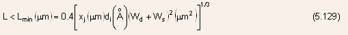
where are the drain-substrate and source-substrate depletion widths respectively.
- This expression indicates the importance of the contact depth,
however, indirectly, this behavior may also by accounted for by a
judicious choice of the adjustable parameter

![]() Model for Mobility
Model for Mobility
- The mobility model, which has gained wide acceptance and is used
almost universally (including BSIM) is given by

where
 is referred to as the low-field mobility, and
  is
referred to as the field-degradation coefficient for mobility.
is
referred to as the field-degradation coefficient for mobility.
-
This is an extremely hot area of research, and lots of work in this area is going on around the world.
-
There are plenty of other models also available in the literature; however, most of these are empirical and based on heuristics.
![]() Hot Electron Effects
Hot Electron Effects
-
As the device sizes are scaled down, the electric field in the channel increases, and, in the saturation region, the high field region near the drain occupies a large fraction of the channel length.
-
This leads to the so-called hot electron effects, which manifest themselves in a superlinear increase in the drain current in the saturation region (the kink effect) and in the degradation of device parameters with time.
- These effects represent a major obstacle to further scaling down
of MOSFET feature sizes.
- The physics of the hot electron effects can be described as follows.
- Electrons, while traveling from source to drain through the channel,
experience a high field near the drain, and acquire large energy.
- When the energy thus acquired by an electron becomes equal to or
greater than the band gap energy, then these electrons can collide
with an atom and create EHPs (impact ionization EHP generation).
- The generated holes are pushed into the bulk due to the electric
field, thus constituting the substrate current, and the electrons
increase the drain current in the saturation region, thus causing
the kink in the drain current characteristics.
- Some of these electrons may even acquire such a large energy from
this field that they can surmount the
 barrier
and get trapped in the oxide => this gives rise to instability
in the device behavior, since these electrons can alter the charge
states in the oxide.
barrier
and get trapped in the oxide => this gives rise to instability
in the device behavior, since these electrons can alter the charge
states in the oxide.
- The process of EHP generation can be described by a generation rate
G, which is an exponential function of the maximum electric field
in the channel
 ,
which is reached at the drain:
,
which is reached at the drain:
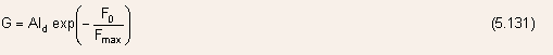
where A is a constant, is
the drain current, and
is
the drain current, and  is
the characteristic field for the impact ionization, given by
is
the characteristic field for the impact ionization, given by  where
where  is
the energy required for an ionization event, and
is
the energy required for an ionization event, and is the mean free path for the ionization process.
 - Typical value of
 is
1.7 mV/cm for Si n-channel MOSFETs.
is
1.7 mV/cm for Si n-channel MOSFETs.
- The generation rate is proportional to the drain current since
it ought to be proportional to the product of the electron sheet density
in the channel and the electron velocity.
-
The maximum electric field is given by
 is
the intrinsic drain-source voltage,
is
the intrinsic drain-source voltage,  is
the intrinsic drain-source saturation voltage, and
is
the intrinsic drain-source saturation voltage, and  is
the length of the pinch-off region, given by
is
the length of the pinch-off region, given by 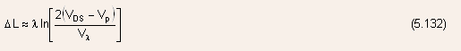
where
 is
the field required for velocity saturation, and
is
the field required for velocity saturation, and is a characteristic length of the electric field variation in the
high field region near the drain and is given by
is a characteristic length of the electric field variation in the
high field region near the drain and is given by 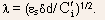
-
The substrate current
 is
proportional to the generation rate, hence,
is
proportional to the generation rate, hence,
where B is a constant

-
Equation (5.133) can be rewritten as
 where
where
- Analysis shows that only one iteration is sufficient to accurately
solve this equation by iteration if
 is
substituted by
is
substituted by  in
Eq.(5.134).
in
Eq.(5.134).
Note: the measured values of Y depend linearly on the drain-source voltage in the kink region, thus, Eq.(5.134) can be used for the extraction of the saturation voltagefrom
the experimental data.
- Hot electrons can also tunnel into traps in the gate oxide near
the drain.
- The negative charge in the oxide causes partial channel depletion
near the drain, leading to an increase in the channel resistance and
a decrease in the threshold voltage in this region.
- Hence, the device characteristics change with time when the drain
voltage is high enough to cause significant electron heating (i.e.,
under voltage stress).
- The increase in the channel resistance should lead to a shift in
the drain-source saturation voltage (it increases) and a reduction
in the drain-source current.
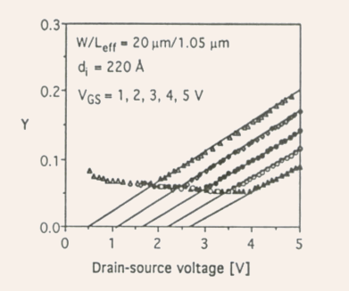
Fig.5.33 Measured Y versus
 curves.
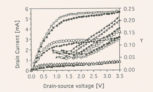
Fig.5.34 -
Measured I-V characteristics and Y-functions for an n-channel Si MOSFET: open symbols data before stress, dark symbols data after stress at
 for
104 sec.
for
104 sec. -
As can be seen from Fig.5.34, the Y versus
curves experience a parallel shift as a result of the voltage stress.
-
This electron trapping also causes a change
 in
the drain current, given by
in
the drain current, given by
where
 is a constant.
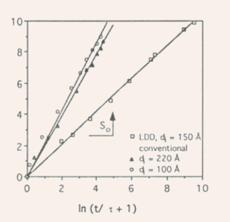
-
Fig.74 Measured values of
 (in
percent) under stress versus time.
(in
percent) under stress versus time.
-
A large number of MOSFET models exist in literature, the most popular among them is the BSIM (Berkeley Short-Channel IGFET Model).
-
Currently, significant research is going on in the area of MOSFET modeling, in order to make these models more accurate in describing device behavior for ultra-short channel length devices.
There are different levels of these models, e.g.
LEVEL 1: Shichman-Hodges
LEVEL 2: Geometric based analytical model
LEVEL 3: Semi-empirical short channel model
LEVEL 4: BSIM
LEVEL 5: New BSIM (BSIM2)
LEVEL 6: MOS6 (Sakurai and Newton)
LEVEL 7: Universal extrinsic short channel model
LEVEL 8: Unified long channel model (UCCM)
LEVEL 9: Short channel model
LEVEL 10: Unified intrinsic short channel model
LEVEL 11: Unified extrinsic a-Si TFT model
LEVEL 12: Polysilicon TFT model
The list given above is by no means complete, and there are plenty more new models, which describe short channel device behavior more accurately than their predecessors.
-
For SPICE simulation, the MOS element is defined in the following way:
-
MX ND NG NS NB MNAME <L=VALUE> <W=VALUE> <AD=VALUE> <AS=VALUE> <PD=VALUE> <PS=VALUE> <NRD=VALUE> <NRS=VALUE> <NRG=VALUE> <NRB = VALUE> <OFF> <IC=VDS,VGS,VBS> <TEMP=T>
where
-
MX is the device number;
-
ND, NG, NS, and NB are the node numbers for the drain, gate, source, and substrate respectively;
-
L and W are the channel length and channel width respectively,
-
AD and AS are the areas of the drain and source respectively,
-
PD and PS are the perimeters of the drain and source respectively,
-
NRD, NRS, NRG, and NRB are the relative resistivities of the drain, source, gate, and substrate respectively in number of squares,
-
OFF indicates an optional initial value for the element in a DC analysis,
- the optional initial value IC=VDS,VGS,VBS is to be used together
with UIC (use initial condition) in a Transient analysis, and the
optional TEMP value is the temperature at which this device operates.
Parameters for LEVELs 1, 2, 3, and 6: