-
The gate-to-drain capacitance
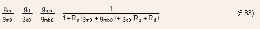
- Note: in the presence of series source/drain resistances
 the
intrinsic (internal to the device) conductance
the
intrinsic (internal to the device) conductance  and
transconductances
and
transconductances  are
related to the extrinsic (measured) transconductances
are
related to the extrinsic (measured) transconductances  and
conductance
and
conductance  by
the following equation:
by
the following equation:
The gate-to-body capacitance ![]()
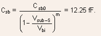
The source-to-substrate capacitance
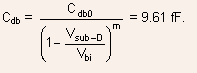
The drain-to-substrate capacitance
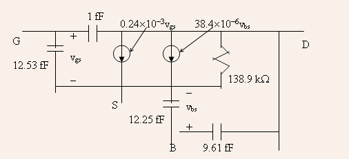
EXAMPLE 5.3: An n-channel MOSFET has ![]() Determine
Determine
![]()
SOLUTION: The intrinsic body transconductance ![]()
The coefficient
Therefore, ![]() and
and
![]() respectively.
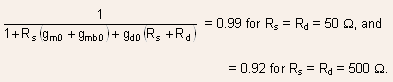
Thus, significant degradation in the transconductances and drain conductance
may take place for large values of source/drain series resistances.
respectively.
Thus, significant degradation in the transconductances and drain conductance
may take place for large values of source/drain series resistances.
- The two conductance terms
 appearing
in the equivalent circuit shown in Fig.5.26(a) are the reverse-bias
conductances of the source-substrate and drain-substrate diodes, and
their values are very small (tending to zero).
appearing
in the equivalent circuit shown in Fig.5.26(a) are the reverse-bias
conductances of the source-substrate and drain-substrate diodes, and
their values are very small (tending to zero).
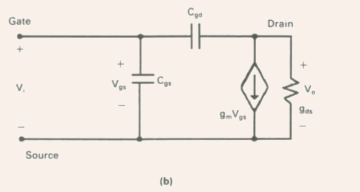
Fig.5.26(b) The simplified equivalent circuit of a MOSFET.
-
A simplified equivalent circuit is shown in Fig.5.26(b).
- For the circuit shown in Fig.5.26(b), the small signal voltage
gain expression can be given by:
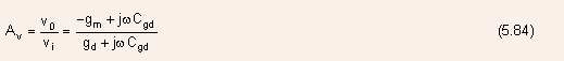
- Note: at low frequencies, when the effects of the capacitances
can be neglected, the voltage gain can be given by
 as
expected.
as
expected.
- Another simplified equivalent circuit, suitable for the calculation
of the current gain, is shown in Fig.5.26(c).
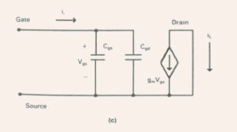
Fig.5.26(c) The alternate simplified equivalent circuit for a MOSFET suitable for the calculation of the short circuit current gain.
-
From Fig.5.26(c), the short circuit current gain can be easily found to be:

-
Thus, the unity gain cutoff frequency (i.e., the frequency at which the absolute value of the short circuit current gain is equal to unity)
 can
be given by
can
be given by
where

-
Now, note that
 in
the strong inversion region.
in
the strong inversion region.
-
Also, the drain current

-
Thus,

-
Hence,
where
 is
the transit time of electrons in the channel.
is
the transit time of electrons in the channel.
-
This equation gives the theoretical maximum value for

-
Assuming
 the
characteristic switching time for a MOSFET is obtained as
the
characteristic switching time for a MOSFET is obtained as 
- In reality, the measured switching times for MOSFETs are at least
several times larger than that predicted above due to the parasitic
and fringing capacitances
 that
has to be added to the gate capacitance
that
has to be added to the gate capacitance  leading
to the following modified expression for :
leading
to the following modified expression for :

EXAMPLE 5.4: Calculate the unity-gain cutoff frequency ![]() for
the MOSFET considered in Example 5.2. Compare this value with theoretical
maximum value for
for
the MOSFET considered in Example 5.2. Compare this value with theoretical
maximum value for ![]() ,
assuming
,
assuming ![]()
SOLUTION: The unity-gain cutoff frequency
![]()
The theoretical maximum value for ![]() =
=![]() = 7.96 GHz.
= 7.96 GHz.
An actual device would show a cutoff frequency, which is smaller
of the two, thus, the actual unity-gain cutoff for the device considered
in Example 5.2 would be 2.82 GHz.
Types of MOSFETs
- Broadly, MOSFETs can be categorized into two types: enhancement and depletion.
- Enhancement type devices are normally off, i.e., channel does not
exist for
 and
the applied
and
the applied  must
be greater than
must
be greater than  for
the device to turn on.
for
the device to turn on.
- On the other hand, depletion type devices are normally on, i.e.,
channel does exist even for
 and
the applied must
be reduced below for
the device to turn off.
and
the applied must
be reduced below for
the device to turn off.
- To put it simply, an n-channel enhancement type device has a positive
,
whereas an n-channel depletion type device has a negative .
- Similarly, a p-channel enhancement type device has a negative ,
whereas a p-channel depletion type device has a positive .
- The threshold voltage can be changed either by doping or by ion
implantation, where high energy ions are made to bombard the surface
and get embedded into it: since these are charged, they can change
the charge state of the surface, and, hence, the threshold voltage.
-
The shift in the threshold voltage
 is
related to the ion density
is
related to the ion density  by
the relation:
by
the relation:  eg.,
negative ions (like Boron) implanted in a p-channel (n-substrate)
device will compensate some of the positive depletion charges and
make the threshold voltage less negative, however, note the same
ions would shift the threshold voltage to more positive for n-channel
(p-substrate) device.
eg.,
negative ions (like Boron) implanted in a p-channel (n-substrate)
device will compensate some of the positive depletion charges and
make the threshold voltage less negative, however, note the same
ions would shift the threshold voltage to more positive for n-channel
(p-substrate) device.
EXAMPLE 5.5: An n-channel MOSFET with ![]() has
a threshold voltage
has
a threshold voltage ![]() Determine
the type and dose
Determine
the type and dose ![]() of
ion implantation required to make it a depletion mode device with
of
ion implantation required to make it a depletion mode device with
![]()
The dose of ion implantation required ![]()
![]()
Since the threshold voltage is shifting towards negative value,
hence, obviously, the type of implant required is positive ions
(e.g., P, As, Sb, etc.), which would compensate the negative depletion
charge of the substrate and push the threshold voltage towards negative
direction.
Some Advanced Models
![]() Unified Charge Control Model for MOSFETs
Unified Charge Control Model for MOSFETs
-
For MOSFETs, the UCCM equation for MIS capacitors [Eq.(4.24)] has to be modified to account for the channel potential, thus, the inversion charge is related to the gate-source and channel potential as follows:

where
 is
the quasi-Fermi (electrochemical) potential measured relative to
the Fermi potential at the source side of the channel, and the parameter
is
the quasi-Fermi (electrochemical) potential measured relative to
the Fermi potential at the source side of the channel, and the parameter
 accounts
for the dependence of the threshold voltage on the channel potential
in strong inversion, and, hence, on the position along the channel.
accounts
for the dependence of the threshold voltage on the channel potential
in strong inversion, and, hence, on the position along the channel.
- In order to get a better understanding of the term first
consider the simplified version of the charge control model, given
by
- Now, in reality, the threshold voltage depends on the depletion
charge.
- Taking into account the dependence of this charge on the channel
potential, one can write the corresponding position dependent threshold
voltage
 as
as
- This makes the charge control equation nonlinear and difficult to use in device modeling.
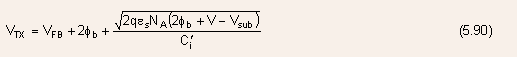
- However, if Eq.(5.90) is linearized with respect to V, one can
write
 where
now
where
now  is
the value of the threshold voltage at the source side of the channel.
is
the value of the threshold voltage at the source side of the channel.
- Thus, one obtains
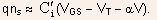
-
A generalized solution for ns is used in UCCM, given by
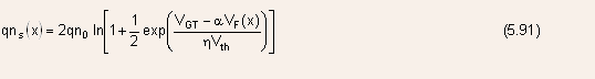
- This equation allows the direct determination of the carrier distribution
along the channel as a function of

![]() Saturation Region: The Region of the Channel with Velocity Saturation
Saturation Region: The Region of the Channel with Velocity Saturation
- Of late, area of considerable interest, since an accurate modeling of the pinch-off region is essential in order to obtain an exact drain current model in saturation.
- Important to find a solution for the longitudinal field in the
channel.
- The model relies on the fundamental assumption that the carrier
velocity in the saturated part of the channel is constant and equal
to the saturation velocity, which implies that the carrier sheet density
in the saturated part of the channel is also constant.
- Another assumption made is that the substrate is lowly doped: this
assumption oversimplifies the true physics of the saturation region,
however, it also leads to a manageable theory with qualitatively correct
features, which gives a fairly good fit to experimental data with
a judicious choice of parameters such as the saturation velocity and
the effective channel thickness.
- The intrinsic saturation voltage
 can
be defined as the intrinsic drain-source voltage
can
be defined as the intrinsic drain-source voltage  for
which the longitudinal electric field at the drain end of the channel
just becomes equal to the saturation field
for
which the longitudinal electric field at the drain end of the channel
just becomes equal to the saturation field 
- For
 the
location in the channel where
the
location in the channel where  marks
the boundary between the saturated and the non-saturated regions.
marks
the boundary between the saturated and the non-saturated regions.
- The boundary point
 moves
towards the source with increasing drain-source voltage: this effect
is called the channel length modulation.
moves
towards the source with increasing drain-source voltage: this effect
is called the channel length modulation.
- Another important parameter is the channel potential at the boundary
point

- The two parameters
 and
on the intrinsic gate-source voltage
and
on the intrinsic gate-source voltage  and
have to be determined self-consistently using the models for the two
regions with the requirement that the potential, the electric field,
and the velocity be continuous at
and
have to be determined self-consistently using the models for the two
regions with the requirement that the potential, the electric field,
and the velocity be continuous at 
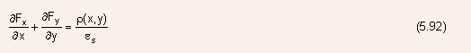
- For a description of the saturated region, it is necessary to consider
a two-dimensional Poisson's equation of the form
| 1 | 2 | 3 | 4 | 5 | 6 | 7 | 8 | 9 | 10 |