- where
 are
the longitudinal and transverse components of the electric field respectively,
are
the longitudinal and transverse components of the electric field respectively,
 is
the semiconductor dielectric permittivity, and
is
the semiconductor dielectric permittivity, and  is
the charge density in the semiconductor
is
the charge density in the semiconductor -
The charge density consists
of a mobile charge density
 and
a depletion charge density
and
a depletion charge density  is
the substrate doping density.
is
the substrate doping density.
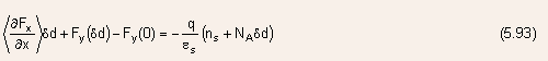
- Integrating Eqn.(5.92) with respect to y from the semiconductor-insulator
interface through the effective channel thickness
 ,
one obtains
,
one obtains - At low substrate doping and with the device biased in strong inversion
such that
 the
vertical electric field at
the
vertical electric field at  will be small compared to the vertical field at the interface, in which
case
will be small compared to the vertical field at the interface, in which
case  can
be neglected in Eqn.(5.93).
can
be neglected in Eqn.(5.93). - Making the substitution
 where
V is the average of the potential over the cross-section of the channel,
Eqn.(5.93) can be written as
where
V is the average of the potential over the cross-section of the channel,
Eqn.(5.93) can be written as
-
The electric field
 at
the interface is obtained by equating the electric displacement at
the two sides of the semiconductor-insulator interface, leading to
at
the interface is obtained by equating the electric displacement at
the two sides of the semiconductor-insulator interface, leading to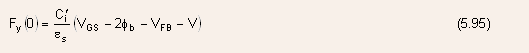
-
From the conditions of velocity saturation and current continuity, the electron sheet density should be a constant in the saturated region, and its value can therefore be determined at the boundary point
 where
the GCA is still valid; thus,
where
the GCA is still valid; thus,
where
 is
the threshold gate voltage, given by Eqn.(5.9).
is
the threshold gate voltage, given by Eqn.(5.9).
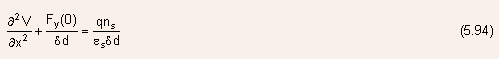
-
The combination of Eqns.(5.94) to (5.96) and (5.9) leads to the following second order differential equation for the channel potential in the saturated region:
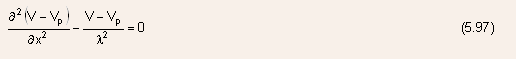
where is the characteristic length in the saturation region and is given by
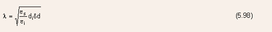
- It should be noted that the solution of Eqn.(5.97) is very sensitive
to the magnitude of the characteristic length
 for the saturated region.
 - In comparisons with experimental data, it is therefore convenient
to treat
as a fitting parameter rather than using Eqn.(5.98), which itself is
a result of rough estimates and approximations.
- The general solution of Eqn.(5.97) can be written in the following
form:
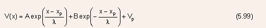
- The coefficients A and B are determined from the boundary conditions,
i.e., from the requirements that
 with
the values
with
the values  respectively,
leading to
respectively,
leading to 
-
A relationship that links
 to
the drain-source voltage is obtained by considering Eqn.(5.99) at
the drain side of the channel:
to
the drain-source voltage is obtained by considering Eqn.(5.99) at
the drain side of the channel:
where
 with
L being the gate length.
with
L being the gate length. -
Equation (5.100) can be solved with respect to
 resulting
in
resulting
in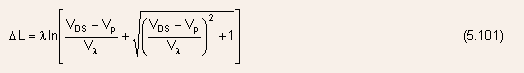
-
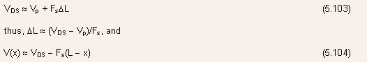
Combining Eqns.(5.99) and (5.101), we find

- A self-consistent determination of
 is
based on a model for the non-saturated part of the channel
is
based on a model for the non-saturated part of the channel - Owing to the complexity of Eqns.(5.99) to (5.101), it is extremely difficult to derive explicit, analytical expressions for important electrical properties, e.g., the I-V characteristics, using the present model for the saturation region.
- However, a numerical solution can readily be obtained which may serve as a physically based reference for simpler, more empirical models.
- Nonetheless, it is possible to simplify the equations somewhat in certain limiting cases.
-
For
 i.e.,
just beyond the onset of saturation, it can be written to the first
order in
i.e.,
just beyond the onset of saturation, it can be written to the first
order in 
-
For
 >
>
 i.e.,
in deep saturation, we have
i.e.,
in deep saturation, we have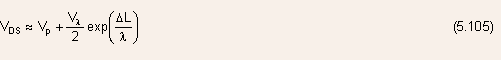
-
From Eqn.(5.105), we obtain
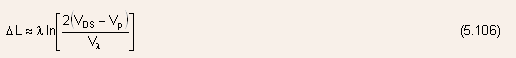
- The solutions obtained represent only an approximation of the actual potential distribution in the saturation region, however, they clearly show that the potential rises exponentially with distance inside this region.
- Based on this result and on numerical simulations of the potential
in the saturation region, a simplified empirical expression linking
the drain-source voltage to the length of the saturation region has
been proposed:
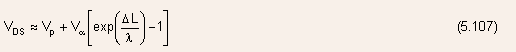
where the constant
 is
determined from the condition of continuity in the drain conductance.
is
determined from the condition of continuity in the drain conductance.
where ![]() over
the channel thickness and
over
the channel thickness and ![]() is
the electron sheet density in the channel.
is
the electron sheet density in the channel.
![]() Subthreshold Region
Subthreshold Region
- Area of considerable research for the last few years due to low-voltage/low-power analog/digital circuit operation, where most of the devices operate very near the threshold region and some may even enter subthreshold operation.
- In the off state of the MOSFET, a finite drain current flows through
the device, since the channel is weakly inverted, and also that there
is a finite injection rate of carriers from the source into the channel.
- In the subthreshold regime in short channel devices, a drain voltage induces lowering of the energy barrier between the source and the channel, this effect is called the drain induced barrier lowering (DIBL) effect.
- DIBL causes excess injection of charge carriers from the source into
the channel, and gives rise to an increased subthreshold current.
- This current is detrimental to both as well as digital operation.
- Figure 5.27 shows qualitatively the band diagram and the potential
distribution at the interface in the channel,

- At the interface, the channel consists of three regions, the source-channel
junction with length
 the
drain-channel junction with length
the
drain-channel junction with length  and
the middle region of length
and
the middle region of length 
- At
 the
interface potential in the middle of the channel
the
interface potential in the middle of the channel  can
be taken to be approximately constant.
can
be taken to be approximately constant.
- A drain-source bias gives rise to a positive contribution V(x) to
the channel potential => the minimum in the interface potential
 will
be localized at the source side of the channel at
will
be localized at the source side of the channel at 
- Associated with the shift in the potential minimum, there will be
a reduction in the interface energy barrier between the source and the
channel by
 this
is the so-called drain induced barrier lowering (DIBL) effect.
this
is the so-called drain induced barrier lowering (DIBL) effect. - DIBL is a short channel effect, which causes a drain voltage induced
shift in the threshold voltage.
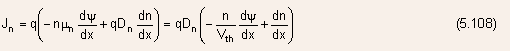
- The expression for the drain current in the drift-diffusion form can be given as
-
where
 is
the potential of the channel region referred to the potential of the
source.
is
the potential of the channel region referred to the potential of the
source.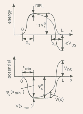
Fig.5.27 Band diagram and potential profile at the semiconductor insulator interface of an n-channel MOSFET. The symmetrical profiles correspond to and
the asymmetrical profiles to
and
the asymmetrical profiles to  The
figure indicates the origin of the Drain Induced Barrier Lowering
(DIBL) effect.
The
figure indicates the origin of the Drain Induced Barrier Lowering
(DIBL) effect. - It is also assumed that the longitudinal electric field in the channel
 is
sufficiently small (except for the junction region near the drain) such
that velocity saturation can be neglected.
is
sufficiently small (except for the junction region near the drain) such
that velocity saturation can be neglected. - Multiplying Eq.(5.108) by the integrating factor
 the
right hand side of this equation can be made into an exact derivative,
and a subsequent integration from source to drain yields (assuming that
the current density remains independent of x):
the
right hand side of this equation can be made into an exact derivative,
and a subsequent integration from source to drain yields (assuming that
the current density remains independent of x):
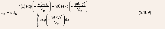
where n(L) = n(0) equals the drain and source contact doping density
 (neglecting
degeneracy).
(neglecting
degeneracy). - With the source contact as the potential reference,
 at
the source end, and
at
the source end, and  at
the drain end, where
at
the drain end, where  is
the intrinsic drain-source voltage.
is
the intrinsic drain-source voltage. - When the device length is not too small, the channel potential can
be taken to be independent of x over a portion of the channel length,
i.e.,
 and
the integral in the denominator of Eq.(5.109) is determined by the contribution
from this portion of the channel.
and
the integral in the denominator of Eq.(5.109) is determined by the contribution
from this portion of the channel. - Note: from Fig.5.27, the length of this section is approximately
equal to
 and
the current density can be expressed as
and
the current density can be expressed as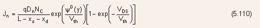
-
For long channel devices,
 and
the drain current can be obtained by integrating the current density
over the cross-section of the conducting channel, thus,
and
the drain current can be obtained by integrating the current density
over the cross-section of the conducting channel, thus,
where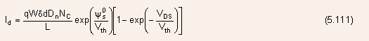
 is
the effective channel thickness, and
is
the effective channel thickness, and  is
the constant potential at the semiconductor-insulator interface, and
is defined relative to the source electrode.
is
the constant potential at the semiconductor-insulator interface, and
is defined relative to the source electrode. - Hence, although the interface potential relative to the interior
of the p-type substrate
 is
the built-in potential between the source contact and the substrate)
is positive,
is
the built-in potential between the source contact and the substrate)
is positive, will be negative for n-channel MOSFETs.
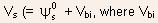
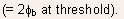
- At threshold, the interface potential in the channel relative to
the source can be expressed as
 is
the potential relative to the interior of the substrate at threshold
is
the potential relative to the interior of the substrate at threshold
- For simplicity, it is assumed that the substrate is shorted to the
source; the effects of a substrate-source bias
 are
found simply by replacing
are
found simply by replacing 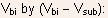 of
course, such a replacement is only valid for negative or small positive
values of ,
a positive comparable
to
of
course, such a replacement is only valid for negative or small positive
values of ,
a positive comparable
to  would
lead to a large substrate leakage current.
would
lead to a large substrate leakage current. - Below threshold, the interface potential can be written as

- All these equations predict that the subthreshold drain current decreases
nearly exponentially with decreasing
 this
current is practically independent of the drain-source voltage.
this
current is practically independent of the drain-source voltage.
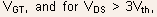
- The effective channel thickness
 is
given by
is
given by
- Note: this expression in only valid when
 i.e.,
in the depletion and weak inversion regions, and this condition is fulfilled
for values of the drain current that are many orders of magnitude smaller
than the threshold current.
i.e.,
in the depletion and weak inversion regions, and this condition is fulfilled
for values of the drain current that are many orders of magnitude smaller
than the threshold current.
- For short channel length devices, L should be replaced by
 as
discussed earlier. 5.9.4 Drain Induced Barrier Lowering (DIBL)
as
discussed earlier. 5.9.4 Drain Induced Barrier Lowering (DIBL) - While dealing with short channel effects, the effective gate depletion charges were distributed evenly along the channel in order to estimate the threshold voltage shift.
| 1 | 2 | 3 | 4 | 5 | 6 | 7 | 8 | 9 | 10 |