- While this may be a good approximation for
 it
will fail to accurately predict the effect on
it
will fail to accurately predict the effect on  of
an applied drain-source voltage.
of
an applied drain-source voltage.
- The reason is that a portion of the additional depletion charge
induced by the drain-source bias will be distributed nonuniformly
from source to drain.
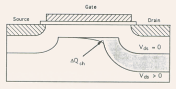
Fig.5.28 Distribution of depletion charge induced by an applied drain-source bias, indicated by the shaded region. is
the part of the induced charge located in the central channel region,
and which has its counter charge on the gate electrode
is
the part of the induced charge located in the central channel region,
and which has its counter charge on the gate electrode -
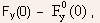
Likewise, the drain-source bias will induce a nonuniform shift V(x) in the interface potential along the channel which increases from V(0) = 0 at the source to
 at
the drain.
at
the drain.
- A model for the distribution of the induced shift V(x) in the interface
potential along the channel as a result of the applied drain-source
bias is required.
- From such a model, it is possible to calculate the interface potential
near its minimum, which defines the barrier for charge injection into
the channel (refer to Fig.5.27).
- An accurate estimate of the shift in the potential minimum is especially
important since the channel current is exponentially dependent on
the barrier height.
- In principle, this involves the solution of a 2-D Poisson's equation
for the whole device, using proper boundary conditions, however, this
requires extensive numerical calculations.
- A simplified analytical calculation is presented below.
- Start by considering the 2-D Poisson's equation for the depletion
region under the gate, away from the source and drain contact depletion
regions.
- In the subthreshold region, the influence of the charge carriers
on the electrostatics of the channel can be neglected, and the 2-D
Poisson's equation can be written as
where
 are
the longitudinal and perpendicular components of the electric field
respectively.
are
the longitudinal and perpendicular components of the electric field
respectively.
- Integrating this equation with respect to y from the semiconductor-insulator
interface through the depletion region yields
where
 is
the average of
is
the average of  over
the thickness of the depletion region, which can be estimated approximately
from a one-dimensional theory as
over
the thickness of the depletion region, which can be estimated approximately
from a one-dimensional theory as
-
The vertical component of the electric field
 at
the semiconductor-channel interface can be found by requiring the
electric displacement to be continuous across the interface, i.e.,
at
the semiconductor-channel interface can be found by requiring the
electric displacement to be continuous across the interface, i.e.,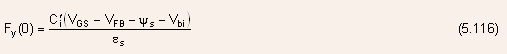
-
In the presence of a drain-source bias, the interface potential can be written as:
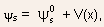 where
where
 is
the constant interface potential of the middle part of the channel
when
is
the constant interface potential of the middle part of the channel
when  and
V(x) is the addition to the channel potential caused by the applied
drain-source voltage.
and
V(x) is the addition to the channel potential caused by the applied
drain-source voltage.
" Away from the source and drain contacts, it can be assumed that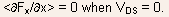
" Now, consider Eq.(5.114) with and without an applied drain-source bias and express the net effect of the drain-source bias by taking the difference, i.e.,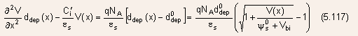
where
 is
the depletion width for V = 0.
is
the depletion width for V = 0.
- In Eq.(5.117),
 is
replaced by
is
replaced by  assuming
that V(x) inside the gate depletion region is relatively weakly dependent
on the distance from the interface
assuming
that V(x) inside the gate depletion region is relatively weakly dependent
on the distance from the interface
- The second term on the left hand side of Eq.(5.117) is equal to
the difference
 where
where
 is
the value of
is
the value of 
- Since both V(x) and its x-derivatives are small outside the depletion region of the drain contact, all terms in Eq.(5.117) can be expanded to first order in V to give
-
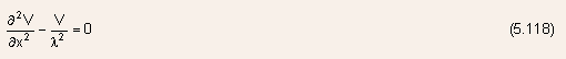
where
-
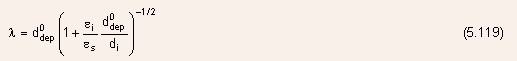
The general solution of Eq.(5.118) can be written as
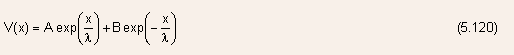
where the coefficients A and B are determined from the boundary conditions.
-
Without much error, one can assume that Eq.(5.120) is also valid through the source-channel junction region
 in
which case one has the boundary condition V(x = 0) = 0, which gives
in
which case one has the boundary condition V(x = 0) = 0, which gives
 such
that Eq.(5.120) can be written as
such
that Eq.(5.120) can be written as

- Here,
 is
a constant that remains to be determined.
is
a constant that remains to be determined.
- Note: the shift
 in
the conduction band at the channel side of the source-channel junction
is identical to the DIBL (refer to Fig.5.27).
in
the conduction band at the channel side of the source-channel junction
is identical to the DIBL (refer to Fig.5.27).
- In order to find the voltage V0, one has to consider the additional
charges induced in the gate electrode and in the substrate as a result
of the applied drain-source voltage.
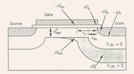
Fig.5.29 Schematic overview of the drain bias induced charges and counter charges according to the principle of charge sharing: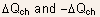 are
the induced charges in the channel and the gate, the remaining charges
and counter charges are those between the drain and the substrate
are
the induced charges in the channel and the gate, the remaining charges
and counter charges are those between the drain and the substrate
 and
between the drain and the gate
and
between the drain and the gate 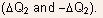
-
In order to be consistent with the potential variation along the channel, calculated earlier, the corresponding sheet charge distribution
 along
the channel has to be as follows:
along
the channel has to be as follows:
where GCA is invoked.
-
Assuming for simplicity that Eq.(5.122) is valid over the range
 the
following expression for is
obtained by requiring that the integral of over
this range equals
the
following expression for is
obtained by requiring that the integral of over
this range equals 
- The induced channel depletion charge
 now
remains to be determined.
now
remains to be determined.
- The shaded region in the substrate in Fig.5.30 indicates roughly
the amount of additional depletion charge
 induced
under the gate by the drain source bias, where
induced
under the gate by the drain source bias, where  is
the depletion width of the drain-channel junction at zero drain-source
voltage.
is
the depletion width of the drain-channel junction at zero drain-source
voltage.
-
From the concept of charge sharing,
can
be taken to some fraction  of
of
 ,
i.e.,
,
i.e.,
where
is
of the order of 0.5, however, the value of this parameter and also
 can
be adjusted to account for the shape and doping profiles in the
drain junction (e.g., lowly doped drain (LDD) MOSFETs) and substrate
(e.g., ion implantation); in other words, this fitting parameter
is technology dependent.
can
be adjusted to account for the shape and doping profiles in the
drain junction (e.g., lowly doped drain (LDD) MOSFETs) and substrate
(e.g., ion implantation); in other words, this fitting parameter
is technology dependent.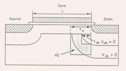
Fig.5.30 Simplified model of the drain bias induced chargein
the substrate under the gate (shown as an estimate of the depletion
charge under the gate between the depletion boundaries for 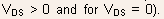 The
induced channel charge
The
induced channel charge  is
a fraction of
according to the charge sharing principle.
is
a fraction of
according to the charge sharing principle. -
The parameter
can
be obtained by substituting Eq.(5.124) into Eq.(5.123), i.e.,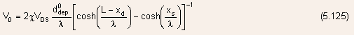
-
Substituting Eq.(5.125) in Eq.(5.121) and setting
 the
lowering of the injection barrier is found to be
the
lowering of the injection barrier is found to be
- Note: The barrier lowering predicted by Eq.(5.126) decreases exponentially
with increasing gate length for

- For sufficiently small gate lengths or sufficiently high drain-source
bias such that
 the
DIBL diverges and Eq.(5.126) is no longer valid => this condition
corresponds to severe punchthrough in the device.
the
DIBL diverges and Eq.(5.126) is no longer valid => this condition
corresponds to severe punchthrough in the device.
- By assuming that the ideality factor does not change significantly
with bias conditions
 the
shift in the interface potential can be evaluated as
the
shift in the interface potential can be evaluated as 
- Thus, as a consequence of the barrier lowering, there will be a
drain bias induced shift in the threshold voltage, given by

where
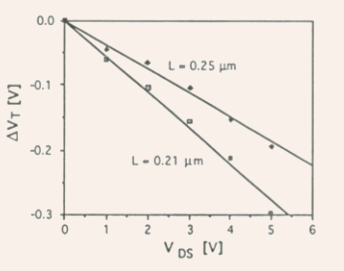
Fig.5.31 Experimentally determined threshold voltage shift as a function of drain-source voltage for two NMOS devices with effective gate lengths of 0.21 and
0.25 .
Equation (5.127) is fitted to the two data sets, yielding
and
0.25 .
Equation (5.127) is fitted to the two data sets, yielding  =
0.056 (L = 0.21 )
and =
0.038 (L = 0.25 ).
=
0.056 (L = 0.21 )
and =
0.038 (L = 0.25 ).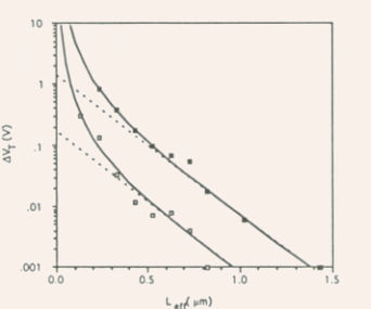
Fig.5.32 Experimental values (symbols), fitted model calculations (solid lines), and exponential approximation (dotted lines) of shift in threshold voltage as a function of effective gate length for T = 85 K (lower curve) and T = 300 K (upper curve). - Note:
 also
varies close to exponentially with
also
varies close to exponentially with 
- Note: an accelerated shift in the threshold voltage is observed
at very small values of
| 1 | 2 | 3 | 4 | 5 | 6 | 7 | 8 | 9 | 10 |