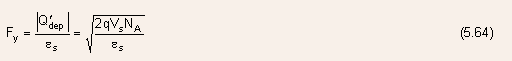
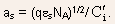
- Similar to the short channel device, the threshold voltage of a
narrow channel (along the width) device increases with a reduction
in the effective device width Weff due to the fringing fields outside
the gate region, and the change in the threshold voltage as a function
of Weff can be given by
where
 is
a constant.
is
a constant.
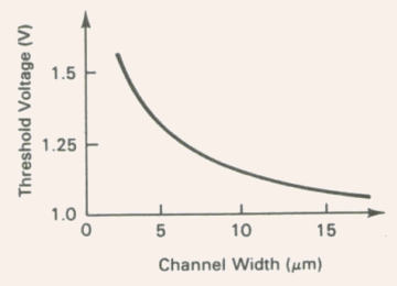
Fig.5.19 Variation of the threshold voltage with the channel width.
-
Another non-ideal effect that may be especially important for
short-channel devices is the injection of electrons from the channel
directly to the gate dielectric, where these electrons get trapped
=> hot electron effect.
-
This phenomenon takes place because the carriers gain sufficient
energy while traversing the drain depletion region, which contains
a high electric field, and has been used to advantage in the FAMOS
(Floating gate avalanche MOS) structures used in memories.
-
Avalanche breakdown of the drain-substrate junction can cause a
sharp increase in the drain current, and can damage the device unless
it is controlled by some external means.
-
Typically, avalanche breakdown for a heavily doped drain-moderately
doped substrate junction takes place at approximately 8 to 10 V.
-
Another very important nonideal and potentially hazardous situation
may arise due to punchthrough, where the drain and source depletion
regions touch each other and cause abnormally large current to flow
through the device: this effect is particularly severe for short
channel devices.
- Punchthrough effect creates a superlinear increase in the drain current with the drain voltage, even at gate voltages below the threshold voltage.
![]() Subthreshold Conduction
Subthreshold Conduction
- So far, we have considered current flow in a MOSFET only when the
gate voltage exceeds the threshold voltage.
- However, in reality, a finite (nonzero) current does flow in a MOSFET even for gate voltages below the threshold voltage, and this effect is more marked for short channel length devices than their long channel counterparts.
- This current is referred to as the subthreshold current, and it
flows for
 when
the surface potential lies between the ranges of the onset of weak
inversion and the onset of strong inversion.
when
the surface potential lies between the ranges of the onset of weak
inversion and the onset of strong inversion.
- The mechanism responsible for subthreshold current is quite different for long-channel and short-channel devices. 5.6.1 Subthreshold Current in a Long Channel Device
- In a long channel device, the situation is similar to a BJT, where the source plays the role of the emitter, the drain is equivalent to the collector, and the substrate is the base.
- The drain voltage drops almost entirely across the drain-substrate
depletion region.
- Thus, the component of the electric field parallel to the
 interface
is small, and the subthreshold current is contributed primarily by
diffusion, just as the case for BJTs.
interface
is small, and the subthreshold current is contributed primarily by
diffusion, just as the case for BJTs.
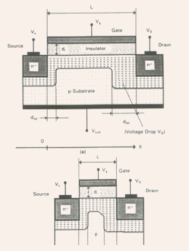
Fig.5.20 The depletion regions associated with a (a) long channel and (b) short channel device.
- Thus, the subthreshold current can be evaluated as

where
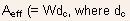 is
the region where most electrons are located) is the effective cross-sectional
area.
is
the region where most electrons are located) is the effective cross-sectional
area.
- The electron density n at the surface is proportional to
 ,
and it decreases with y (perpendicular to the interface)
proportionally to
,
and it decreases with y (perpendicular to the interface)
proportionally to 
where is
the vertical electric field, given by
is
the vertical electric field, given by
- Thus, the effective depth
 where
most of the electrons are concentrated, can be estimated as
where
most of the electrons are concentrated, can be estimated as  where
y = 0 corresponds to the interface.
where
y = 0 corresponds to the interface.
- If the diffusion length of electrons in the substrate
 is
much greater than the channel length L, then the electron density
n should be a linear function of x, decreasing from the source towards
the drain (just like the linear distribution of minority carriers
in the base of a BJT):
is
much greater than the channel length L, then the electron density
n should be a linear function of x, decreasing from the source towards
the drain (just like the linear distribution of minority carriers
in the base of a BJT):
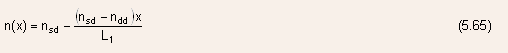
where the volume concentrations for electrons
 at
the source and the drain sides of the channel are given by
at
the source and the drain sides of the channel are given by
where V(y) is the potential given by
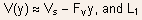 is
the length of the undepleted portion of the channel.
is
the length of the undepleted portion of the channel.
- For long channel devices, it is assumed that the depletion widths
at the source and the drain sides of the channel are small compared
to the channel length L, and

- Also, note that since

- Using all the relations given above, the subthreshold current for
a long channel MOSFET can be given by

- The surface potential
 at
the source can be expressed as a function of the gate voltage by noting
that
at
the source can be expressed as a function of the gate voltage by noting
that  thus,
thus,

where
- Note: For
 the
subthreshold current becomes independent of the drain voltage.
the
subthreshold current becomes independent of the drain voltage.
- This is expected since in a long channel device, most of the applied drain voltage drops at the drain-substrate depletion region, and since the current is diffusive in nature, there is no change in the current with the drain voltage.
- Also, for large
 since
since
 the
gradient of n is not affected by the drain voltage: a situation similar
to BJTs, where the collector current in the forward active mode is
independent of the collector-to-emitter voltage.
the
gradient of n is not affected by the drain voltage: a situation similar
to BJTs, where the collector current in the forward active mode is
independent of the collector-to-emitter voltage.
- Note: the subthreshold current is almost independent of the drain
voltage

- The substrate bias shifts the threshold voltage to a more positive
value, affects the surface potential, and thus the subthreshold current
changes.
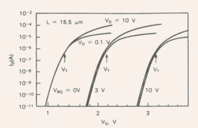
Fig.5.21 The subthreshold characteristics for a long channel device as a function of the gate voltage for different values of drain and substrate voltages.
![]() Subthreshold Current in a Short Channel Device
Subthreshold Current in a Short Channel Device
- In a short channel device, the source and drain depletion widths
 may
be a significant portion of the channel length L, and, hence, can
not be neglected.
may
be a significant portion of the channel length L, and, hence, can
not be neglected.
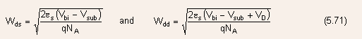
- To account for this effect, the term L in Eq.(5.67) is replaced
by another term Leff, where
 where
where
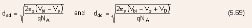
where
 is
the built-in voltage of the
is
the built-in voltage of the  source/drain-substrate
junction, and the surface potential
source/drain-substrate
junction, and the surface potential  is
now found from the solution of the following equation:
is
now found from the solution of the following equation: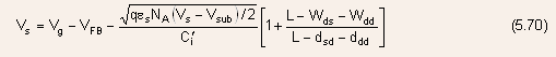
where
- The curves clearly show shifts in the subthreshold current for different values of drain voltages, a characteristic typical of short channel devices.
- The subthreshold current is a strong function of temperature as
well
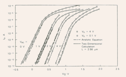
Fig.5.22 The subthreshold characteristics for a short channel device as a function of gate voltage for different values of drain and substrate voltages.
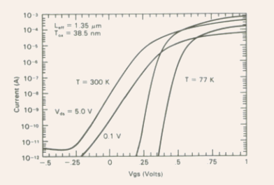
Fig.5.23 The subthreshold characteristics as a function of gate voltage for two different temperatures (77 K and 300 K).
![]() MOSFET Capacitances and Equivalent Circuit
MOSFET Capacitances and Equivalent Circuit
- Note: in a MOSFET, the charges in the depletion region and the
inversion layer depend on the gate, source, drain, and substrate potentials;
and the derivatives of these charges with respect to the terminal
voltages give rise to MOSFET capacitances.
- The small signal equivalent circuit shown in Fig.5.24 is the one
used by the popular circuit simulation package called SPICE, and it
contains:
- the drain-to-source current source IDS,
- two resistances
 (due
to the quasi-neutral region resistances of the source and drain respectively)
(due
to the quasi-neutral region resistances of the source and drain respectively)
| 1 | 2 | 3 | 4 | 5 | 6 | 7 | 8 | 9 | 10 |