![]() Short Channel and Nonideal Effects in MOSFETs
Short Channel and Nonideal Effects in MOSFETs
- For long channel devices, the drain current becomes constant in
saturation, whereas, for short channel devices, the drain current
increases continuously with the drain-to-source voltage.
Fig.5.15 I-V characteristics of two n-channel MOSFETs: (i) L = 0.5 (dashed
lines), and (ii) L = 0.75 (solid
lines).
(dashed
lines), and (ii) L = 0.75 (solid
lines).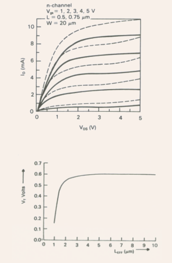
Fig.5.16 The variation of the threshold voltage with the effective channel length.
- Another interesting feature seen in short channel devices is that
the saturation current increases as the device length is reduced.
- Now, based on the existing model for the threshold voltage, which states that it is independent of the device length this behavior cannot be explained.
- In reality, it has been shown that the threshold voltage is a strong function of the channel length (for short channel devices), and it actually decreases with a decrease in the channel length, which explains the reason behind the larger saturation current.
- The reduction of the threshold voltage with a reduction in the
channel length can be explained by the charge sharing model.
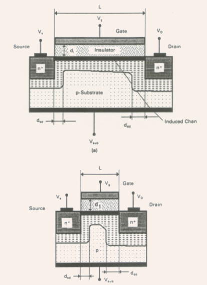
Fig.5.17 The depletion charge profiles for (a) a long channel device, and (b) a short channel device.
- For a long channel device, the depletion layer thickness
 at
the source end of the channel and
at
the source end of the channel and  at
the drain end of the channel are much less than the channel length
L, and, thus, the depletion charge enclosed by these sections are
much smaller than the total depletion charge under the gate.
at
the drain end of the channel are much less than the channel length
L, and, thus, the depletion charge enclosed by these sections are
much smaller than the total depletion charge under the gate.
- However, for a short channel device, the widths of these depletion
regions are a non-negligible fraction of the total depletion charge
under the gate.
- Note: essentially, the depletion regions near the source and the
drain are contributed by the source-substrate and the drain-substrate
bias, and gate has no role to play.
- Under an applied drain-source bias, the depletion region thickness
near the drain will obviously be larger than that at the source side.
- The net effect is that the gate now has to compensate for a lower
depletion charge density than that for a long channel device, which
qualitatively explains the reduction of the threshold voltage with
a reduction in the channel length.
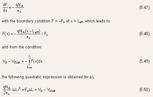
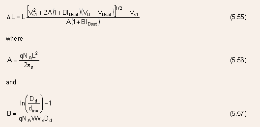
- The exact analysis of the charge sharing effects requires a two-dimensional
analysis, however, to the first order, it is assumed that the effect
of the depletion width at
the drain side of the channel is to reduce the effective channel length
in the saturation region from L to
 where
where

- Here,
 is
the effective channel length, and the voltage dropped along this section
is assumed to be equal to the drain saturation voltage
is
the effective channel length, and the voltage dropped along this section
is assumed to be equal to the drain saturation voltage  ,
and
,
and  is
length of the pinched-off portion of the channel (related to the drain
depletion width), where the excess drain voltage beyond ,
i.e.,
is
length of the pinched-off portion of the channel (related to the drain
depletion width), where the excess drain voltage beyond ,
i.e.,  is
dropped, where
is
dropped, where  is
the applied drain voltage.
is
the applied drain voltage.
- With an increase in
 the
length of the pinch-off region also
increases, leading to a reduction in the effective channel length
.
the
length of the pinch-off region also
increases, leading to a reduction in the effective channel length
.
- This effect is called the channel length modulation effect, and
this effect leads to a higher drain saturation current, and finite
output conductance
 in
the saturation region.
in
the saturation region.
- A very crude estimate of the pinch-off length
(also referred to as the drain region length) can be obtained from
the solution of the one-dimensional Poisson's equation:
- A more accurate and realistic expression for may
be obtained by assuming that the electrons are injected from the inversion
layer into the drain depletion region, and they spread uniformly,
leading to the current density
- Here,
 is
the diffusion depth of the
is
the diffusion depth of the  drain
region, and
drain
region, and  is
the thickness of the inversion layer
is
the thickness of the inversion layer 
- It is also assumed that the velocity of electrons in this region
is saturated, thus their volume density can be given by

- Now, the one-dimensional Poisson's equation can be rewritten as:
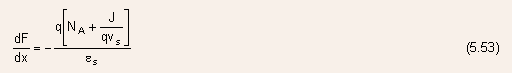
- The solution of this equation leads to the following complicated
expression for :
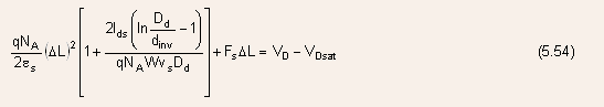
- For gate lengths larger than or about 1 ,
and drain-to-source voltages smaller than or about 10 V, this expression
may be simplified to give
- In short channel devices, the depletion charge under the channel
[dependent on the channel potential and has been represented by the
second term within the brackets in the right-hand side of Eq.(5.7)],
which has been neglected in the charge control model [Eq.(5.19)],
has to be accounted for.
- This effect may be taken into account by introducing an additional
parameter a into the equations of the charge control model, with the
resulting equations given by
-
Linear Region

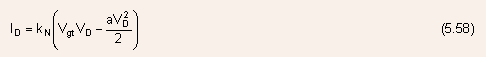
-
Saturation Region

- For Si, the (empirical and fitting) parameter a describes the influence
of the bulk substrate depletion layer on the device characteristics,
and can be approximated by the following expression
- The threshold voltage
 and
the parameter K can be determined from the experimentally measured
data for a given device.
and
the parameter K can be determined from the experimentally measured
data for a given device.
-
In addition, the dependence of electron mobility on the longitudinal and transverse electric field in the channel should be included for a more realistic device modeling, however, this simple empirical model gives adequately good fit with the measured data.
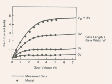
Fig.5.18 The measured and calculated I-V characteristics for a Si n-channel MOSFET.
| 1 | 2 | 3 | 4 | 5 | 6 | 7 | 8 | 9 | 10 |