- Note: from the constancy of the drain current
 throughout
the device, it can be seen that as
throughout
the device, it can be seen that as 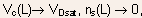 and
the electric field F(L) diverges.
and
the electric field F(L) diverges.
- The differential drain conductance
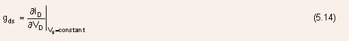
tends to zero when
 and
the I-V characteristics may be extrapolated in the voltage region
and
the I-V characteristics may be extrapolated in the voltage region
 assuming
a constant (independent of
assuming
a constant (independent of  drain
current
drain
current 
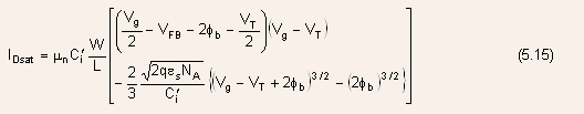
-
 may
be found by substituting
may
be found by substituting  from
Eq.(5.8) into Eq.(5.7), which results in a highly complicated expression,
however, it can be simplified for gate voltages close to the threshold
voltage
from
Eq.(5.8) into Eq.(5.7), which results in a highly complicated expression,
however, it can be simplified for gate voltages close to the threshold
voltage 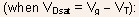
- Note: this approach is only valid when the channel electrons do
not suffer any velocity saturation due to high electric fields.
- Note: modern day MOSFETs have extremely small gate lengths, and
the channel has high electric fields (more than the critical electric
field required for velocity saturation), which creates the velocity
saturation effects for the channel electrons.
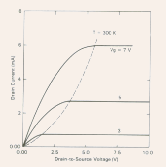
Fig.5.7 The I-V characteristics of an n-channel MOSFET for different values of gate voltage .
The dashed line represents the drain-to-source saturation voltage.
.
The dashed line represents the drain-to-source saturation voltage.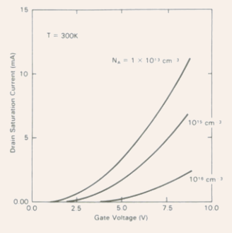
Fig.5.8 The variation of the drain saturation current with gate voltage for three different values of substrate doping. - For very small
 the
terms under the curly brackets in Eq.(5.15) can be expanded in Taylor
series, leading to the following simplified expression for the I-V
characteristics in the linear region:
the
terms under the curly brackets in Eq.(5.15) can be expanded in Taylor
series, leading to the following simplified expression for the I-V
characteristics in the linear region:
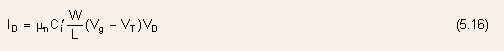
- A physical justification of Eq.(5.16) can be given as follows:
- At very small the
charge induced in the channel is, to the first order, independent
of the channel potential, thus,
(5.17)
- Now, for small the
electric field F in the channel is nearly constant, and is
given by
-
The drain current is entirely due to drift, and is given by the electrons in transit model:

since

5.2.3 The Charge Control Model
- A simplified description of the I-V characteristics of a MOSFET
can be obtained by using the charge control model.
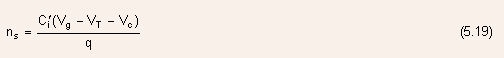
- In this model, it is assumed that the concentration of free carriers
induced in the channel is given by
- Compare Eq.(5.19) with Eq.(5.2): in Eq.(5.19), the variation of
the depletion charge density
 with
the channel potential has been neglected.
with
the channel potential has been neglected.
- The drain current
 can
now be given by
can
now be given by

- Compare Eq.(5.20) with Eq.(5.5).
- Equation (5.20) can be rewritten as
- Integrating Eq.(5.21) from x = 0 (source side) to x = L (drain
side), which corresponds to a change in
 from
from
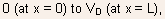 the
following expressions for the I-V characteristics are obtained:
the
following expressions for the I-V characteristics are obtained:
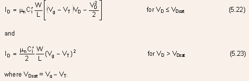
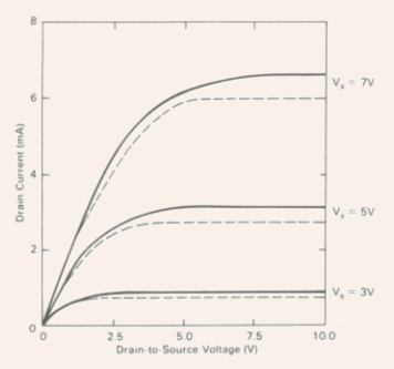
Fig.5.9 The I-V characteristics of an n-channel MOSFET calculated using the charge control model (solid curve) and the Shockley model (dashed curve).
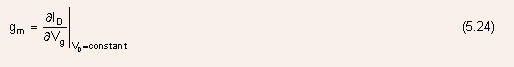
- The differential transconductance
 is
defined as
is
defined as
- From Eqs.(5.22) and (5.23),
where
 is
referred to as the device transconductance parameter, with
is
referred to as the device transconductance parameter, with  is
referred to as the process transconductance parameter.
is
referred to as the process transconductance parameter.
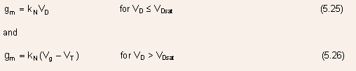
- Thus, in order to achieve a high value for the transconductance
gm, the following steps may be taken.
- Higher value of low field electron mobility

- Thinner gate dielectric layers, which in turn gives large values
for the insulator capacitance per unit area
- Large widths (W) and short lengths (L).
- Note: for short channel devices, where velocity saturation effects are important, the dependence of transconductance on the low-field electron mobility and the gate length gets strongly affected.
EXAMPLE 5.1: An n-channel MOSFET with the process transconductance
parameter ![]() the
threshold voltage
the
threshold voltage ![]() is
biased at
is
biased at ![]() Determine
the drain current ID, the transconductance
Determine
the drain current ID, the transconductance ![]() and
the drain conductance
and
the drain conductance ![]()
SOLUTION:
Hence, the device is under linear mode of operation
.
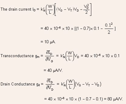
Note the huge change in transconductance in saturation as compared to the linear region: this is due to the square law dependence of current on the gate voltage in the saturation region (as against the linear variation in the linear region).
Drain Conductance ![]()
This is due to the independence of the saturation drain current on
the drain voltage. In reality, channel length modulation creates a change
in drain current with respect to the drain voltage in saturation, and
finite drain conductance ![]()
![]() Effect of Source and Drain Series Resistance
Effect of Source and Drain Series Resistance
-
The analysis so far neglects the effects of the source/drain series resistance, and the entire voltage is assumed to drop along the channel.
- However, for modern day MOSFETs, this effect cannot be ignored,
due to smaller diffusion cross-sections and smaller drain currents.
- The extrinsic (measured) voltages
 can
be related to the intrinsic (device) voltages
can
be related to the intrinsic (device) voltages  by
the following equations:
by
the following equations:
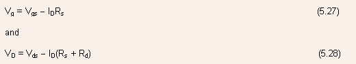
where
 are
the source and drain resistances respectively.
are
the source and drain resistances respectively.
- The extrinsic transconductance
 is
related to the intrinsic transconductance
is
related to the intrinsic transconductance 
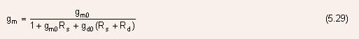
where
 is
the intrinsic drain conductance.
is
the intrinsic drain conductance.
-
Similarly, the extrinsic drain conductance
 is
related to the intrinsic drain conductance
is
related to the intrinsic drain conductance 
| 1 | 2 | 3 | 4 | 5 | 6 | 7 | 8 | 9 | 10 |