3. Structural Testing With Internal Memory: An Example Of A 32 Bit Adder
A 32-bit adder shown is Figure 4 requires 232 test patterns for exhaustive functional testing. As discussed in last section, structural testing of the 32-bit adder can reduce the testing time to a great extent. In this case, we consider a full adder as one structural unit (like the AND gates for the circuit in Figure 2). The implementation of the 32-bit adder in terms full adders (i.e., structural units) is also shown in Figure 4. Now we illustrate how structural testing of the 32-bit adder can be done with only 8(=23 ) test patterns and 3 extra pin outs. The 32-bit adder with DFT circuitry is shown in Figure 5.
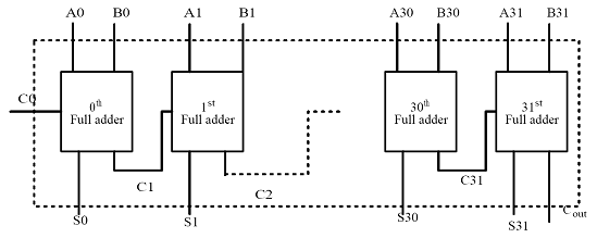
Figure 4. A 32-bit adder
The DFT circuitry comprises, 2 31-bit shift registers, 31 2-1multiplexers and 3 pin outs. One shift register (called input register) provides inputs to the ``carry input'' bits of the individual adders during test and the other shift register (called output register) latches outputs from the ``carry output'' bits of the individual adders. In the modified 32-bit adder, the carry input to the i th (full) adder is multiplexed with the i th -bit of the input shift register, 1≤ i ≤ 31. During normal operation of the 32-bit adder, the multiplexers connect the carry input of the i th (full) adder to the carry output of the ( i-1) th (full) adder, 1≤ i ≤ 31. However, during test, the multiplexers connect the carry input of the i th (full) adder to the output of the i th -bit of the input shift register, 1≤ i ≤ 31 . The values in the shift register are fed externally. It may be noted that by this DFT arrangement all the (full) adders can be controlled individually as direct access is provided to the carry inputs of the adders; inputs other than carry are already controllable. Hence, testing in this case would be for each (full) adder individually and that requires 8 test vectors as each of the 32 full adders can be tested in parallel.
Correct operations of each of the full adders are determined by looking at the sum and the carry outputs. Sum outputs are already available externally and hence no DFT circuit is required to make them directly observable. For the carry outputs, however, another similar DFT arrangement is required to make them observable externally. This would require the output (31 bit parallel load and) shift register where the carry output bit of the ( i-1) th adder is connected to the i th input of the output shift register, 1≤ i ≤ 31. Once the values of all the carry bits are latched in the register, which is done in parallel during test, they are shifted out sequentially. In this case a full adder is tested functionally and structural information is used at the cascade level.
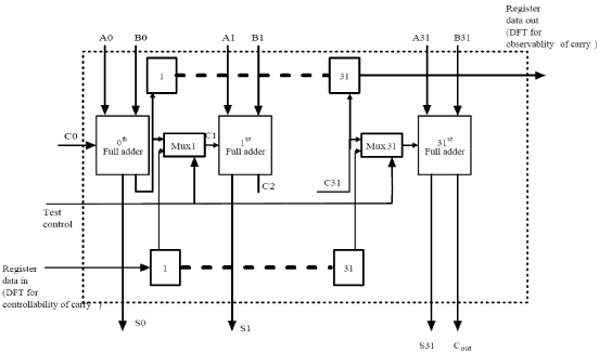
Figure 5. A 32-bit adder with DFT circuitry