2. Repeat similar test patterns for all the 5 input AND Gates G2, G3, G4, G5 and G6.
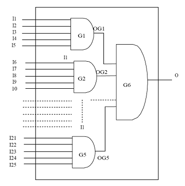
Figure 2. Gate level implementation for Bit wise ANDing circuit
So number of test patterns required are 6.25 So number of test patterns required are 6.25 (=160), which is many fold smaller than those required for functional testing (225). In this case, time required for testing the circuit the using a 1 Mega Hz Tester is 0.000016 seconds and for a million samples is 16 seconds. Now we can easily see the benefits for structural testing over functional testing. However, some piece is to be paid for the benefits obtained, as listed below
- Each individual gate is tested; however, the integration is not tested. From history of several thousand cases of chips being fabricated and tested, it was observed that the quality of test solution given by structural testing is acceptable.
- To test the individual gates, controlling and observing values of intermediary nets in a circuit becomes mandatory, which adds to extra pins and hardware. For example, to test Gate G1 (for circuit shown in Figure 2) we need to apply signals at pins I1 through I5 which are primary inputs and brought out of the chip as pins. But we also need to observe the output at net OG1, which is difficult as it is not a primary output and is internal to the chip. So, for structural testing, involving testing of Gate G1 individually, OG1 is to be brought out of the chip as a special output (test) pin. Similarly for individual testing of the gates G2 through G5, lines OG2 through OG5 are to be made observable by additional pin outs. So for structural testing some internal nets are to be made observable by extra pin outs.
- Now for testing G6, the problem is different. The output of the gate G6 can be observed as it is a primary output. However, to test G6, inputs are to be given through internal nets OG1 through OG5. It may be noted that these nets are outputs of other AND gates and to drive these nets directly to a required value, not only they are to be brought out of the chip as pins but also are to be decoupled from the corresponding AND gates. So for structural testing some internal nets are to be made controllable by extra pin outs and circuitry. Controllability is achieved by adding extra 2-1 Multiplexers on these nets. This is illustrated in Figure 3 (as bold lines boxes). During normal operation of the circuit the Test Mode signal (i.e., connected to select lines of the 2-1 Multiplexers) is made 1; the outputs of the AND gates (G1-G5) are passed to the inputs of the AND gate G6. When G6 is to be tested, Test Mode signal is made 0; inputs to Gate G6 are decoupled from Gates G1 through G5 and now they can be driven directly by additional input pins TI1 through TI5. These additional circuits (Multiplexers and pins) to help in structural testing are called Design for Testability (DFT).
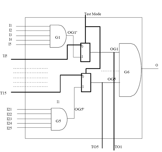
Figure 3. Extra pins and hardware for structural testing of circuit of Figure 2.
It is to be noted that a circuit with about a million internal lines needs a million 2-1 Multiplexers and same number of extra pins. This requirement is infeasible. So let us see in steps how these problems can be minimized, yet maintaining quality of test solution. In the next section we illustrate using an example, to show internal memory can reduce extra pin outs for DFT.