Step 5: Test Planning
As discussed, in VLSI designs millions of transistors are packed into a single chip, thereby leading to manufacturing defects. So all chips need to be physically tested by providing input signals from a pattern generator and comparing responses using a logic analyzer. As in the case of verification, testing by applying all possible input combinations is prohibitive, due to curse of dimensionality problem. The testing problem is more time hungry than verification because all chips need to be tested while only “one” design is to be verified. Testing by applying all possible input combinations is called exhaustive functional testing, which is avoided because of prohibitive time requirements.
Testing is therefore done based on “structure” of the circuit and is called structural testing. In structural testing we first decide on set of faults that can occur, called Fault Models; stuck-at, bridging etc. are some well known fault models. Then we apply only those inputs which are required to validate that faults (as per fault model) are not present. It has been shown in [9] that number of patterns required to perform structural testing is exponentially lower than that required for exhaustive functional testing. In Test Planning step, given a logic level circuit and fault model, we generate patterns, which when applied to a circuit determines that no fault from the fault model exists in the circuit.
Now we will illustrate test planning for the adder module of the example (Figure 8) assuming that fault model is “stuck-at”. In “stuck-at” fault model each line of the circuit is assumed to have two types of faults i.e., stuck-at-0 and stuck-at-0. So if there are n lines in a circuit then in all there can be 2n stuck-at faults in the circuit. However, in the fault model it is assumed that only one stuck-at fault can occur at a time. In test planning we need to find input patterns which can determine that none of the stuck-at faults are present. In the circuit of Figure 8 as there are 12 lines (9 lines in circuit for “sum” and 3 lines in the circuit for “carry”), there can be 24 stuck-at faults. We take one fault at a time and determine an input pattern that can verify the absence of the fault. Here we will illustrate for only one fault and the same holds for all the other 23 faults. Let there be a stuck-at-0 fault in the output of one AND gate (shown in Figure 9) of the circuit for “sum”. Now to we need to find an input pattern that can verify the absence of the fault i.e., when the pattern in applied the output under normal and fault cases are different. Form Figure 9 it may be noted that if a=1 and b=0 is applied as inputs, then “output1(sum)” is 0 if fault is present, 1 otherwise. So a=1 and b=0 can verify the absence of fault by comparing output with 1.
It may be the fact that one pattern can test more than one fault and one fault can be tested by more than one pattern. Broadly speaking, determination of minimal test patterns which cover all faults is the most important step in test planning. Algorithms and techniques to perform test planning will be covered in “TESTING” part of the course.
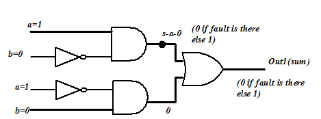
Figure 9. Detection of s-a-0 fault in the circuit for “ Out1(sum)”
Step 6: Fabrication, Testing and Marketing.
Once all the steps from 1 through 5 are completed and verification after each level of transformations are done, the chips are fabricated, physically tested and fault free chips are sent for marketing.
The flow discussed above has been kept simple for introduction. In reality there are iterations back and forth, especially between any two adjacent steps, and occasionally even remotely separated steps. Although top-down design flow provides an excellent design process control, in reality, there is no truly unidirectional top-down design flow. Both top-down and bottom-up approaches have to be combined. For instance, if a chip designer obtained an RTL circuit from specifications (using HLS tools) without estimation of the corresponding chip area, then it is very likely that the resulting chip layout exceeds the area limit. In such a case, in order to fit the architecture into the allowable chip area, the HLS design process must be repeated. Thus, it is very important to feed forward low-level information to higher levels (bottom up) as early as possible.
Further, details and integrities of the steps are also avoided. For example, there are some faults which cannot be tested by any pattern. For such cases, we need to put additional circuitry to make it testable called Design for Testability (DFT).
The respective modules in this course will elaborate on each of these aspects.