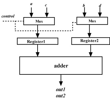
Figure 5. Block diagram with control modules added after allocation and binding
The HLS tool generates output comprising, (i) operations-variables allocated-binded to hardware units and (ii) control modules. The output of HLS tool is called Register Transfer Level (RTL) circuit because data flow, data operations and control flow are captured between registers. After HLS, RTL circuits are transformed into logic gate level implementation; the step is called logic synthesis.
Before the starting of logic synthesis, one needs to verify if the RTL is equivalent to the specifications. In the running example, we can verify by applying all possible input conditions of a,b,c,d (along with control , if RTL is as per Figure 5) to the RTL and checking if out1 and out2 are as expected. However, if the RTL has about hundreds of inputs then exercising all possible inputs is impossible because of the exponential complexity (i.e., if there are n inputs then all possible input combinations are 2n). So we need to have formal verification methods which verify equivalence of RTL with input specifications. Broadly speaking, for formal verification we need to model the RTL circuit and the specifications using some formal modeling techniques and verify that both of them are equivalent. In other words, equivalence is determined without applying inputs. Figure 6 illustrates Control and Data Flow Diagram (CDFG) [4], a formal modeling, to capture the RTL of Figure 5.In Figure 7 we illustrate a Finite State Machine (FSM) [4] to model the control logic of the RTL of Figure 5. This example being very simple, we can see that both specifications and the model are equivalent. Formal techniques for checking equivalence can be found in [5] and will be elaborated in “VERIFICATION” section of the course.
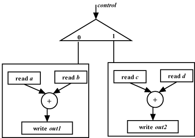
Figure 6. CDFG of the RTL circuit of Figure 5
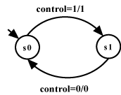
Figure 7. FSM for the control logic of RTL circuit shown in Figure 5