Now depending on availability of hardware resources and time constraints the scheduled operators and variables are allocated and binded to hardware units. Let there be one adder and two registers in the library. So the two operations (addition) of the example, even if scheduled in one control step, cannot be allocated to the single adder. Similarly, the four variables cannot be allocated to two registers. In the running example with the given resource constraints, the two operations can be done in two control steps: Step 1- variable a is allocated to Register1, variable b is allocated to Register2 and operation “out1=Register1+Register2;” is allocated to adder; Step 2- variable c is allocated to Register1, variable d is allocated to Register2 and operation “out2=Register1+Register2;” is allocated to adder. Figure 3 illustrates allocation and binding (of variables and operations) for the running example when there is one adder and two registers in the library.
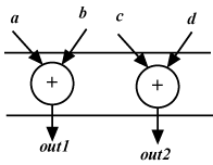
Figure 2. Scheduling of the operations for the example
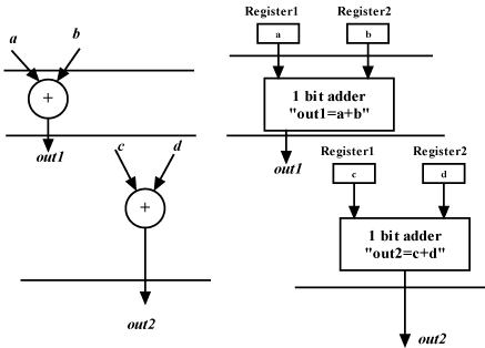
Figure 3. Allocation of operators and variables to hardware units ( 1 adder + 2 Registers)
However, if there are two adders and four registers in the library then both the operations can be carried out in one control step. Figure 4 illustrates binding of variables and operations for the running example for such a case.
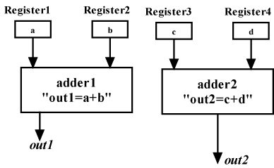
Figure 4. Allocation of operators and variables to hardware units (2 adders + 4 Registers)
Finally, based on allocation and binding, the control unit is to be designed (at high level) in this step. If the allocation/binding is according to Figure 4, the control is trivial. However, if the allocation is according to Figure 3, then the control circuit needs to provide signals that can do multiplexing between a and c, b and d; in 1 st control step, a should be fed to Register1 and b should be fed to Register2, while, in 2 nd control step, c should be fed to Register1 and d should be fed to Register2. Figure 5 illustrates the block diagram where control modules are added after allocation and binding (Figure 3). It may be noted that control signal is not available as an external pin which can be controlled by the user. “ Control” is connected to some signal generated by the system, which alternates in every control step thereby making its value 0 in 1 st step and 1 in the 2 nd .