Lecture 28 : Basics Of DRAM Cell And Access Time Consideration
29.4 Metal Gate Diffusion Storage
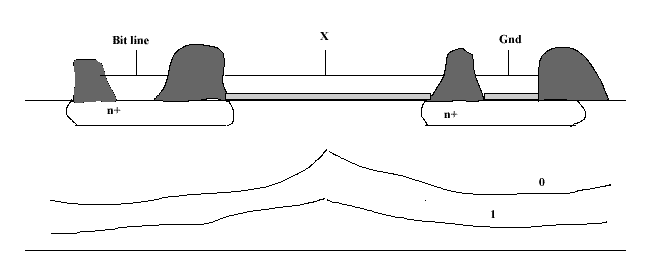
The cross section of a Metal Gate Diffusion Storage is shown below in Figure 29.41.
Fig 29.41: Metal Gate Diffusion Storage
In this case the charge is stored in the depletion capacitance of the substrate and diffusion region. The problem with this design are:
Diffusion line has higher capacitance. Thus increases and hence CTR decreases.
Parasitic capacitances are higher and the gate is not self-aligned.
There is routing problem associated with this kind of design.
A very much similar configuration can be used for inversion storage. In this case when gate input goes HIGH, the inversion charge stored in the capacitor is drained out and the potential at the channel drops indicating a '1' was stored. The reverse phenomena occurs if a '0' is stored.
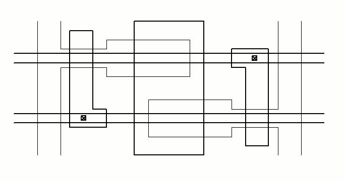
Several DRAM cells are in place now. Few of them are as follows: