Lecture 29 : Basics Of DRAM Cell And Access Time Consideration
29.3 DRAM Read Process With Dummy Cell
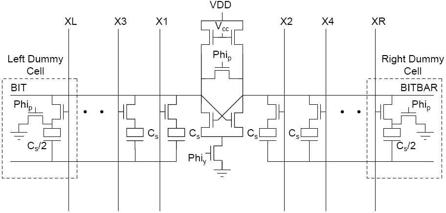
Circuit Construction:
The circuit is illustrated in Figure 29.31. Each bit line is split into two identical halves. Each half line is connected to half cells in the column and an additional cell known as Dummy cell having a capacitor . When a word line on the left side is selected for reading the Dummy cell on the right side (controlled by XR) is also selected and vice versa, i.e. when a word line on the right side is selected the Dummy cell on the left (controlled by XL) is also selected. In effect, then, the Dummy cell operation serves as the other half of a differential DRAM cell. When the left bit line is in operation, the right half bit line acts as Complement for b line and vice versa. These cells shown here are the cells of a column, but look like a row. The distribution of the select lines are such that the even X's are in the right half and all the odds are in the left half.
Fig 29.31: Arrangement for obtaining differential operation from the single ended DRAM cell