Lecture 29 : Basics Of DRAM Cell And Access Time Consideration
29.2 Differential Operation In Dynamic RAMs
The sense amplifier responds to difference in signals appearing between the bit lines. It is capable of rejecting interference signals that are common to both lines, such as those caused by capacitive coupling from the word lines. For this common-mode to be effective, both sides of the amplifier must be matched, taking into account the circuit that feed each side. This is required in order to make the inherently single ended output of the DRAM cell appear differential.
Single To Differential Conversion:
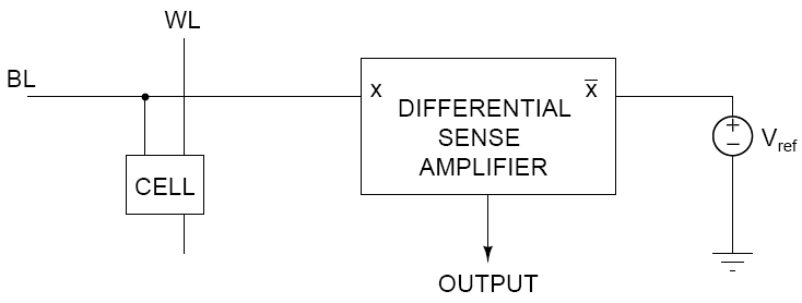
Large memories (>1Mbit) that are exceedingly prone to noise disturbances resort to translating the single ended sensing problem into a differential one. The basic concept behind the single to differential is demonstrated in Figure 29.21
Fig 29.21: Single to differential conversion
A differential sense amplifier is connected to a single ended bit line on one side and a reference voltage positioned between the "0" and "1" level at the other end. Depending on the value of BL the flip flop toggles in one or the other direction. Voltage levels tend to vary from die to die or even a single die so the reference source must track those variations. A popular way of doing so is illustrated in Figure 29.31 for the case of 1T DRAM. The memory array is divided into two halves, with the differential amplifier placed in the middle. On each side, a column called Dummy cell is added, these are 1T memory cells that are similar to the others, but whose sole purpose is to serve as reference. This approach is often called Open bit line archiecture.