Lecture 28 : Basics Of DRAM Cell And Access Time Consideration
29.5 Calculation Of Change In Bitline Voltage
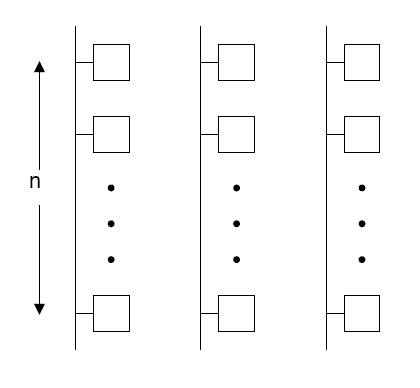
An array of DRAM cells is laid out as in Figure 29.21
Fig 29.21: Array of DRAM Cells
Let the capacitance per unit length of bitline be and the storage capacitance of the DRAM cell be . If there are n such sections (as shown) then the net bit capacitance of the bitline is .
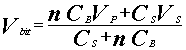
Let the bitline be precharged to . So when the bitline is connected to the capacitance of the DRAM cell, the net voltage will be some intermediate voltage due to charge sharing and is given by:
(Eq 29.1)
A term Charge Transfer Ratio is defined in this context as
(Eq 29.2)
where is defined as .
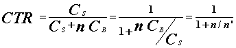
For a particular technology, is fixed. So only can be changed. When the bitline is connected to storage capacitor, the change of voltage at the bitline is given by
(Eq 29.3)
For good design the value of (the change in voltage at bitline) should be as high as possible, so that it will allow the sensor to sense the bit correctly and quickly. Increase in requires CTR to increase. That leads to increase in the value of . depends on and . Thus to increase the storage capacitance can be increased or the bitline capacitance can be decreased or both can be done. However increasing the value of storage capacitance requires larger area.