Lecture 29 : Basics Of DRAM Cell And Access Time Consideration
29.4 Operation Of The Read Circuit
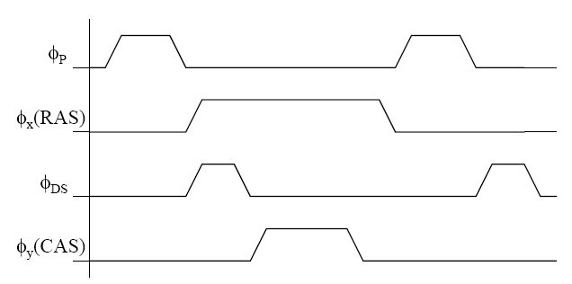
The circuit is shown in the previous slide in Figure 29.31. The two halves of the line are precharged to and their voltages are equalized. At the same time, the capacitors of the two Dummy cells are precharged to . Then a word line is selected, and the Dummy cell of the other side is enabled (with and raised to ). Thus the half line connected to the selected cell will develop a voltage increment (above ) of v or v0 depending on whether a "1" or "0" is stored in the cell. Meanwhile the other half of the line will have its voltage held equal to that of (i.e. ) the result is a differential signal that the sense amplifier detects and amplifies when it is enabled. As usual by the end of the regenerative process, the amplifier will cause the voltage on one half of the line to become and that on the other half to become 0.
Fig 29.41: Timing diagram of DRAM operation
If X1 cell is accessed, then the dummy cell on the right side is also selected.
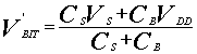
Then the actual voltage of the bit line will be , where
where is BIT capacitance and is storage cell capacitance. is voltage between the nodes of the storage capacitance. The storage capacitance with dummy cell is taken on both sides in a column.
If
then ; this shows that there is no charge sharing.
If
then ;
Since Dummy cell is discharged
(which is between 5 and 4)
The tricky part of a DRAM cell lie in the design of the circuitry to read out the stored value and the design of the capacitor to maximise the stored charge/minimise the storage capacitor size. Stored values in DRAM cells are read out using sense amplifiers, which are extremely sensitive comparators which compare the value stored in the DRAM cell with that of a reference cell. The reference cell used is a dummy cell which stores a voltage halfway between the two voltage levels used in the memory cell (experimental multilevel cells use slightly different technology). Improvements in sense amplifiers reduce sensitivity to noise and compensate for differences in threshold voltages among devices.
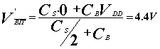 (which is between 5 and 4)