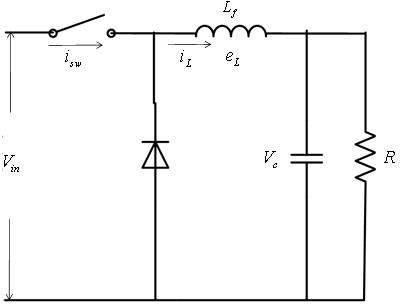
The Buck Converter with R Load and Filter
The output voltage and current of the converter contain harmonics due to the switching action. In order to remove the harmonics LC filters are used. The circuit diagram of the buck converter with LC filter is shown in Figure 6 . There are two modes of operation as explained in the previous section.
The voltage drop across the inductor in mode 1 is
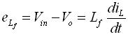 and
and ![]() (25)
(25)
where iL is the current through the inductor Lf
isw is the current through the switch
The switching frequency of the converter is very high and hence, iL changes linearly. Thus, equation 25 can be written as
![]() (26)
(26)
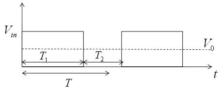
where Ton is the duration for which the switch S remains on
T is the switching time period
|
|
Figure 6: Buck converter with resistive load and filter |
Figure 7: Voltage and current waveform |
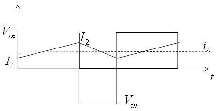
Hence, the current ripple ![]() is given by
is given by
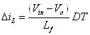 (27)
(27)
When the switch S is turned off, the current through the filter inductor decreases and the current through the switch S is zero. The voltage equation is
![]() (28)
(28)
where iD is the current through the diode D
Due to high switching frequency, the equation 28 can be written as
![]() (29)
(29)
where Toff is the duration in which switch S remains off the diode D conducts
Neglecting the very small current in the capacitor Cf , it can be seen that
![]() for time duration in which switch S conducts
for time duration in which switch S conducts
and
![]() for the time duration in which the diode D conducts
for the time duration in which the diode D conducts
The current ripple obtained from equation 29 is
![]() (30)
(30)
The voltage and current waveforms are shown in Figure 7 .