Module 3 : Fabrication Process and Layout Design Rules
Lecture 12 : CMOS Fabrication Technologies
 
12.4 N-well Technology (contd.)

We now return to the generalized fabrication sequence of n-well CMOS integrated circuits. The following figures illustrate some of the important process steps of the fabrication of a CMOS inverter by a top view of the lithographic masks and a cross-sectional view of the relevant areas.


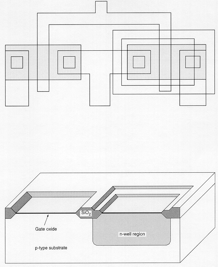
The n-well CMOS process starts with a moderately doped (with impurity concentration typically less than 1015 cm-3) p-type silicon substrate. Then, an initial oxide layer is grown on the entire surface. The first lithographic mask defines the n-well region. Donor atoms, usually phosphorus, are implanted through this window in the oxide. Once the n-well is created, the active areas of the nMOS and pMOS transistors can be defined

 
image
 

The creation of the n-well region is followed by the growth of a thick field oxide in the areas surrounding the transistor active regions, and a thin gate oxide on top of the active regions. The two most important critical fabrication parameters are the thickness and quality of the gate oxide. These strongly affect the operational characteristics of the MOS transistor, as well as its long-term stability.


back
9
next