Module 3 : Fabrication Process and Layout Design Rules
Lecture 12 : CMOS Fabrication Technologies
 
12.4 N-well Technology

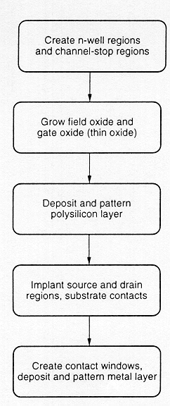
In this discussion we will concentrate on the well established n-well CMOS fabrication technology, which requires that both n-channel and p-channel transistors be built on the same chip substrate. To accomodate this, special regions are created with a semiconductor type opposite to the substrate type. The regions thus formed are called wells or tubs. In an n-type substrate, we can create a p-well or alternatively, an n-well is created in a p-type substrate. We present here a simple n-well CMOS fabrication technology, in which the NMOS transistor is created in the p-type substrate, and the PMOS in the n-well, which is built-in into the p-type substrate.

 
Historically, fabrication started with p-well technology but now it has been completely shifted to n-well technology. The main reason for this is that, "n-well sheet resistance can be made lower than p-well sheet resistance" (electrons are more mobile than holes).
 

The simplified process sequence (shown in Figure 12.41) for the fabrication of CMOS integrated circuits on a p-type silicon substrate is as follows:

  • N-well regions are created for PMOS transistors, by impurity implantation into the substrate
  • This is followed by the growth of a thick oxide in the regions surround the NMOS and PMOS active regions.
  • The thin gate oxide is subsequently grown on the surface through thermal oxidation.
  • After this n+ and p+ regions (source, drain and channel-stop implants) are created.
  • The metallization step (creation of metal interconnects) forms the final step in this process
simpProcessSteps
Fig 12.41: Simplified Process Sequence For Fabrication Of CMOS ICs
 

The integrated circuit may be viewed as a set of patterned layers of doped silicon, polysilicon, metal and insulating silicon dioxide, since each processing step requires that certain areas are defined on chip by appropriate masks. A layer is patterned before the next layer of material is applied on the chip. A process, called lithography, is used to transfer a pattern to a layer. This must be repeated for every layer, using a different mask, since each layer has its own distinct requirements.


back
5
next