Module 3 : Fabrication Process and Layout Design Rules
Lecture 12 : CMOS Fabrication Technologies
 
12.4 N-well Technology (contd.)

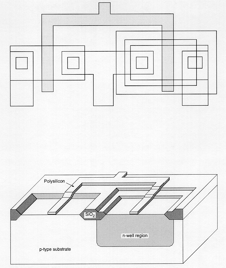
Chemical vapor deposition (CVD) is used for deposition of polysilicon layer and patterned by dry (plasma) etching. The resulting polysilicon lines function as the gate electrodes of the nMOS and the pMOS transistors and their interconnects. The polysilicon gates also act as self-aligned masks for source and drain implantations.


The n+ and p+ regions are implanted into the substrate and into the n-well using a set of two masks. Ohmic contacts to the substrate and to the n-well are also implanted in this process step.

 
image


back
10
next