Module 3 : Fabrication Process and Layout Design Rules
Lecture 12 : CMOS Fabrication Technologies
 
12.4 N-well Technology (contd.)
In this section, we will examine the main processing steps involved in fabrication of an n-channel MOS transistor on a p-type silicon substrate.
 

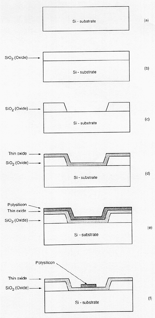
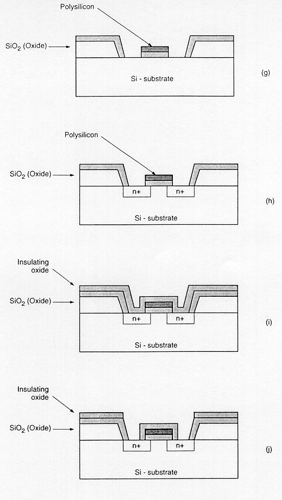
The first step of the process is the oxidation of the silicon substrate (Fig 12.44(a)), which creates a relatively thick silicon dioxide layer on the surface. This oxide layer is called field oxide (Fig. 12.44(b)). The field oxide is then selectively etched to expose the silicon surface on which the transistor will be created (Fig. 12.44(c)). After this the surface is covered with a thin, high-quality oxide layer. This oxide layer will form the gate oxide of the MOS transistor (Fig. 12.44(d)). Then a polysilicon layer is deposited on the thin oxide (Fig 12.44(e)). Polysilicon is used as both a gate electrode material for MOS transistors as well as an interconnect medium in silicon integrated circuits. The resistivity of polysilicon, which is usually high, is reduced by doping it with impurity atoms.


Deposition is followed by patterning and etching of polysilicon layer to form the interconnects and the MOS transistor gates (Fig. 12.44(f)). The thin gate oxide not masked by polysilicon is also etched away exposing the bare silicon surface. The drain and source junctions are to be formed (Fig 12.44(g)). Diffusion or ion implantation is used to dope the entire silicon surface with a high concentration of impurities (in this case donor atoms to produce n-type doping). Fig 12.44(h) shows two n-type regions (source and drain junctions) in the p-type substrate as doping penetrates the exposed areas of the silicon surface. The penetration of impurity doping into the polysilicon reduces its resistivity. The polysilicon gate is patterned before the doping and it precisely defines the location of the channel region and hence, the location of the source and drain regions. Hence this process is called a self-aligning process.


The entire surface is again covered with an insulating layer of silicon dioxide after the source and drain regions are completed (Fig 12.44(i)). Next contact windows for the source and drain are patterned into the oxide layer (Fig. 12.44(j)). Interconnects are formed by evaporating aluminium on the surface (Fig 12.44(k)), which is followed by patterning and etching of the metal layer (Fig 12.44(l)). A second or third layer of metallic interconnect can also be added after adding another oxide layer, cutting (via) holes, depositing and patterning the metal.

 
imageimage  
image
Fig 12.44: Process flow for the fabrication of an n-type MOSFET on p-type silicon


back
8
next