Other data transfer bindings to interconnects can be interpreted in a similar manner from Figure 2.
It may be noted that as two data transfers (point 1 and point 2, above) are binded to regsiter1, we need a multiplexer that feeds to the input of register1. Similarly, we require a multiplexer at input of register3. It may be noted that even if two data transfers “reading b from input bus” and “reading c from input bus” are binded to register2, there is no multiplexer at input of register2. This is because we connect the input line to register2, where in step1 we have value of b and in step2 we have value of c. For a similar reason we do not require a multiplexer for input of register4.
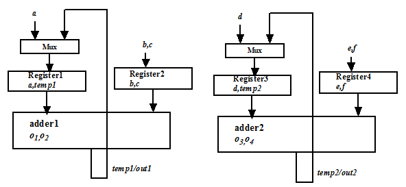
Figure 2. Case 1 of Binding for the schedule shown in Figure 1
So for the binding case illustrated in Figure 3, interconnect binding adds two multiplexers in the circuit.
Let us consider the another option of binding (shown in Figure 3):
- Operations 01,04 are binded to adder1
- Operations 02,03 are binded to adder2
- Variables a,temp2,out1 are binded to register1
- Variables b,f are binded to register2
- Variables d,temp1,out2 are binded to register3
- Variables e,c are binded to register4
The interconnects are illustrated in Figure 3 and can be interpreted in a similar manner as discussed for the last case. It may be noted that in this case also we require two multiplexers in the circuit.
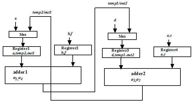
Figure 3. Case 2 of Binding for the schedule shown in Figure 1Now, let us consider the third option of binding (shown in Figure 4):
- Operations 01,04 are binded to adder1
- Operations 02,03 are binded to adder2
- Variables a,temp1,out2 are binded to register1
- Variables b,f are binded to register2
- Variables d,temp2,out1 are binded to register3
- Variables e,c are binded to register4