1. Introduction
In the last (double) lecture we disused scheduling algorithms, which is the first step in HLS. After the scheduling process, which assigns control steps to all the operations, in the allocation step, circuit modules from the design library are selected for executing the operations. Once circuit modules are selected, binding is done, which accomplishes the following:
- Functional unit binding: All arithmetic and logic operations (like addition, division, comparison etc.) are binded to the specific circuit modules allocated from the design library.
- Storage to register binding: A storage operation is created for each data transfer that crosses a control step boundary. In other words, when a functional unit computes an operation and the result is to be stored for use in future control step, then the result of the operation is to be stored in a variable which is to be binded (stored) to a register. Also, all inputs are to be stored in variables and binded to registers.
- Data-transfer to interconnect binding: Any data transfer involves an interconnection between source and sink e.g., after computation data transfer involves interconnection between an operator (source) and a register (sink). Therefore, any data transfer is to be binded with an interconnection (from source to destination). In addition, it might be noted that interconnects are shared by data transfers which leads to use of multiplexers in the sources and destinations.
In the next section, we will give a simple example to illustrate these three sub-parts of the binding task. Following that, we will discuss algorithms that automate the binding procedure.
2. Illustrative Example: Binding of functional units, storages and data-transfer
A schedule of expressions “out1=a+b+c” and “out2=d+e+f” is shown in Figure 1. Let the allocation be as follows:
- Two (ripple carry) adders
- Four registers (D-flip-flops)
We need two adders because in control step1 (also in step2) two addition operations are scheduled and each need an adder to operate. Also we need four registers because in step1, we need four variables (storage) namely, a,b,c,d. These four registers can be re-used in step2 for variables temp1,c,temp2,f.
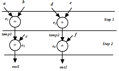
Figure 1. Schedule of expressions “out1=a+b+c” and “out2=d+e+f”
Let us consider the following option of binding (shown in Figure 2):
Operations 01, 02 are binded to adder1
- Operations 03, 04 are binded to adder2
- Variables a,temp1,out1 are binded to register1
- Variables b,c are binded to register2
- Variables d,temp2,out2 are binded to register3
- Variables e,f are binded to register4
The interconnects are illustrated in Figure 2. Some of the binding of the data-transfers with the interconnects are as follows:
- adder1 to register1 (via Mux) is binded to data transfer “temp1=a+b”
- Input a to register1 (via Mux) is binded to data transfer “reading a from input bus”
- Input b (and c) to register2 (via Mux) is binded to data transfer “reading b from input bus” (“reading c from input bus”)