4. CDFG: Control flow based representation and Data flow based representation
CDFG can be control flow based or data flow based. In this section, we will illustrate these two types of representations using an example of a Verilog code; the code is shown in Figure 8. The Verilog code involves some computations over inputs B,C and D depending on value of “ cond ”.

Figure 8. Verilog code having case statement
The control flow based CDFG for the code is shown in Figure 9. The CDFGs discussed in the last section were control flow based ones. From Figure 9 it may be noted that for each value of “ cond ” there is a sub-sequence of operations represented by storage and operational nodes. Here, the operations are classified based on three values of “ cond ”: 00, 01, default (10,11) and the corresponding sub-sequence of operations involving storage and operational nodes are enclosed by three squares. Therefore, the control flow based CDFG has almost a one to one mapping with the lines of Verilog code. So, control flow based CDFG gives an idea that, depending on value of condition of a control node (“ cond ” in this cond ”. So, three hardware circuitry are to be kept in the chip and depending on the value of “ cond ”, the output of appropriate circuitry would write “A”. In other words, unlike a software code, where parts of a code can be invoked based on values of a condition, in hardware, all the different types of circuitry are to be implemented in the chip (and would be executed) and the output being used depends on the value of a condition.
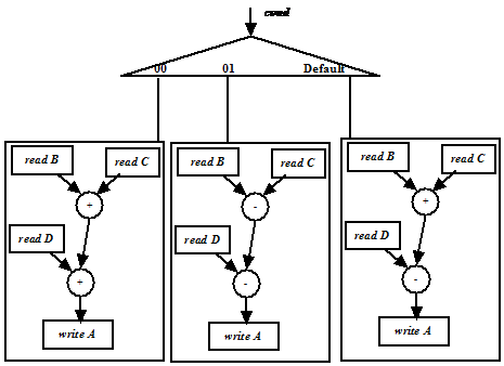
Figure 9. Control flow based CDFG for Verilog code of Figure 8
CDFG that uses the above-mentioned concept of hardware is called data flow based representation. Figure 9 illustrates data flow based CDFG for Verilog code of Figure 8. It may be noted that in this case, the control node is after the operational and storage nodes. There are three circuits for computing different values of “A" , depending on “ cond ”. The three circuits evaluate three different outputs irrespective of the value of “ cond ”; “A” is written by the output of the appropriate circuit depending on value of “ cond ”. It may also be noted that even if three different circuitry are required to compute different possible values of “A”, many operational and storage nodes are common among these circuits and redundancy can be eliminated. For example, reading of B,C,D are required by all the three circuits and they may be implemented by storage nodes common to all the three circuits. Also, operational node for “B+C” is common to circuit for “A = B + C + D” and circuit for “A = B + C - D”, which can be merged.