The CDFG for “for loop” in Verilog is shown in Figure 4. The CDFG has a storage node (B1) which holds the variable on which the loop executes. It also has an operational node that compares variable with constant (or any other variable) to decide execution/exit of the loop. The output of this operational node feeds a control node (C1) which decides data flow direction after the condition is checked. Finally, the graph has two other operational nodes (B3 and B4) which correspond to data flows from the control node.
From the discussion, it is clear that CDFGs are quite coherent with HDLs and can be easily built from hardware specifications. In this lecture, we will not discuss on other HDL statements (which can be built in a similar way as discussed above), for details, the reader is refereed to [4].
3. CDFG with timing
Sometimes minimum required delay needs to be mentioned in the specifications. Delay information is required in logic synthesis. Delay of a circuit depends on gates and architecture. For example, speed of ripple-carry adder is lower compared to carry-look-ahead adder; however, area of carry-look-ahead adder is higher than ripple-carry adder. Also, faster gates consume more area and power compared to slower gates. So, if tolerable delay of some operation in a circuit is low (which depends on application), realizing it with faster circuitry unnecessarily leads to high area and power overheads. In CDFG, delay information is modeled using a node between the required points, where the delay is specified. The points can be between single operational nodes (shown in Figure 5), between multiple operational nodes (shown in Figure 6), loop (shown in Figure 7) etc.
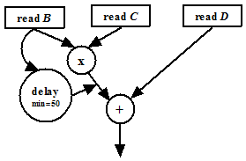
Figure 5. CDFG with timing requirements between a single operational node
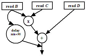
Figure 6. CDFG with timing requirements between multiple operational nodes
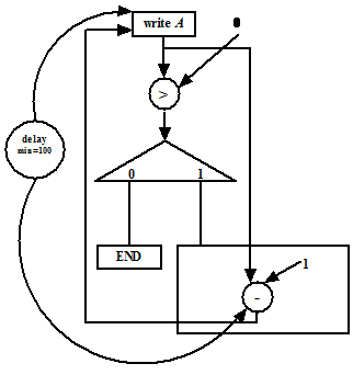
Figure 7. CDFG with timing requirements in loops