3. Alignment:
For most of the layers in lithography, alignment to another layer is necessary. For example, in order to make a metal line correctly, it has to be aligned to the previous layer (via layer) which connect the bottom layer to the top layer. The metal line which is printed on the top should align exactly with the bottom layer. Otherwise the connection will not function.
In ideal situation, everything will align perfectly. However, in practice the alignment will not be perfect and there will be some misalignment. If the line widths and spaces are of the size of say 65 nm, then the alignment tolerance is probably in the range of 10 nm. i.e. We would like it to align perfectly with the previous layer, but a 10 nm misalignment is tolerable. Thus even if the lines are off by 10 nm, they will conduct and the chip will function. Beyond 10 nm, this will lead to problems and ultimately to the failure of the chip.
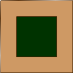
Box in Box alignment mark
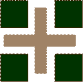
Cross alignment mark
Figure 2.17 a and b. Example alignment marks
The alignment is made using standard marks called alignment marks. A few examples are given in fig 2.17 a and b. Figure 2.17 a is called “box in box” (i.e. one box would be at the bottom layer and there will be a box on the mask of the top layer). These marks are sometimes called “Fiducials”. The machine will align the box in the mask such that it will exactly fall at the center of the other box. Another example, shown in fig 2.17 b, is called cross. In this case, a cross will be there on the mask and it must be aligned to fall exactly within the four square marks present in the previous layer. These marks are usually present at the corners and edges of the masks.(Please see the next paragraph for relevant details)
4. Partial field and full field
The last topic that is important in manufacturing is the issue of partial field. Normally, a mask will not have only one chip. One chip may be of 3 mm x 5 mm size, but a mask can be much larger. Then one mask will have multiple copies of a chip (see figure 2.18). The large box is the mask. The smaller boxes represent the chips. The gaps between the chips, and the border areas are used for keeping alignment marks. During the lithographic process, one exposure of this mask is called “field” or “shot”. The alignment marks are actually placed in the ‘gaps’ between the chips or at the corners of the field.
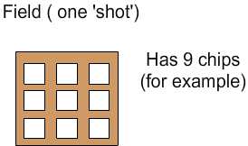
Figure 2.18. Example “field” or “shot”
Two questions arises right away. 1. “Why not make the mask very large and make hundred chips in it?” 2. “On the other hand, why not make a small mask with only one chip?”
We cannot make the mask very large because the size of the lens is not unlimited. For very large lenses, the cost becomes very high. Beyond a limit, we cannot make the lens very large even if money is not a constraint. Thus, the size of the mask is limited by the size of the lens that we can make.
It is possible to make a small mask containing only one chip. However, one has to remember that in the lithographic process, the printing is done step by step. i.e. the mask is brought on top of wafer, aligned to one spot and light is switched on for a controlled time. Then the mask is moved on to the next part, aligned, exposed and so on. So, it is a time consuming process. During production, through put, (i.e. the number of chips produced per hour, or number of wafers processed per week) has to be high. The lithography equipment are very expensive, of the order of Rs. 5 crores (in 2010), and one cannot afford to buy too many of these equipment. Hence, it is necessary to maximize the utilization and minimize the time spent per wafer in these expensive machines. In one exposure or “shot”, if many chips can be made, then the total time will be saved. We also know that we cannot make a very large mask because of limitations on the size of lens. So, one makes the mask of the maximum acceptable size based on lens limitations, and within that, fit as many chips as possible. In this example, it is nine chips.
With this background, we will look into the issue of partial field. The wafer is a circular piece, but a mask is a rectangular piece. It is obvious that in most exposures, all the nine chips square can be fitted into the wafer very nicely, but near the wafer edge, some of the chips will fall outside the wafer. These exposures are called “partial fields”.
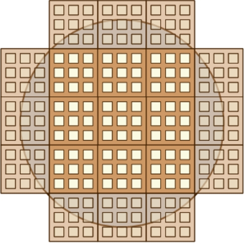
Figure 2.19. Partial fields and full fields in a wafer
In the figure 2.19, for convenience, different colors are used to show the full field and partial fields separately.
What is the problem with partial field? First, when we align the mask to the previous layer, we use the alignment marks, which will be on all four corners of the mask (field). In partial field, only one or two corners will fall within the wafer and the rest will be outside the wafer. There is no “previous layer” outside the wafer and hence the alignment has to be done with only one or two marks, which makes it difficult. Second, the focusing is done automatically by the equipment for all exposures. In full field, all the image will fall on the wafer while in partial field, part of the image falls outside the wafer. This makes it difficult for the equipment to focus and this leads to poor image quality.
Just because partial field is problematic, one can not leave these areas empty. It is a useful wafer area. Also, we saw that presence or absence of a line will affect lithography process and that it can be corrected using OPC. Similarly, the presence or absence of patterns will affect neighboring areas. i.e. If partial field areas are left as blank, it will affect the neighboring full field also during the subsequent process. Thus it is better to expose these areas also so that these areas will have at least some images even if they are not perfect images. The alignment and focusing algorithm used by the machine can be modified to control the partial field shots better. One can also optimize the position to some extent, but beyond that not much can be done. There will always be some area which falls in the partial fields. One should be aware of this when they estimate the yields for the production of a particular chip. The details of yield will be discussed in the later chapter.
EUV and X Ray lithography
The very recent lithography process which, in 2011, is in the pilot stage (i.e. before mass production) is called Extreme Ultra Violet (EUV) lithography. It is expected to be used for 22 nm technology (i.e. when the gate length is 22 nm). It uses electromagnetic waves at 13.5 nm. Any electromagnetic wave of wavelength in the range of 10 nm to 400 nm is called UV. The waves of 10 to 120 nm wavelength are called Extreme UV. These are generated using plasma sources. Since almost all materials absorb EUV, the EUV lithography must be done in vacuum. The mask and other optics would be using reflective method and not refractive (normal lens system) method. Another technique in research mode is X-ray lithography. Since X-rays have very short wavelengths (less than 1 nm), the diffraction limitations of normal lithography would not be present. Some of the difficulties faced are (a) it is difficult to bend and focus the X-rays and hence only 1X mask can be used and (b) secondary electrons generated by X-ray causes contrast issues. Since most dust particles will transmit X rays, particle contamination is less of an issue. Interestingly, X ray lithography is applied in micro electro mechanical system (MEMS) fabrication. A problem common to all next generation techniques is that they are very expensive.
Immersion Lithography: In the latest commercial lithographic instruments (as of 2012), a technique called liquid immersion lithography is used. In this, a fluid such as water (or preferably with high refractive index) is introduced between the wafer and the lens, as shown in Fig. 2.20. If the refractive index of the fluid matches that of the lens, (and assuming that the refractive index of the photoresist is similar to that of the lens) then the images formed at the bottom of the photo resist will be with high resolution. Comparatively, if the fluid were not present, the light path will be different and the resolution will be poorer. Even if the refractive index of the fluid is not the same as that of the lens, if it is higher than that of air, it will enhance the resolution. The resolution enhancement obtainable through immersion lithography is about 30 to 40% and an increased depth of focus (40 to 70%) can also be achieved.
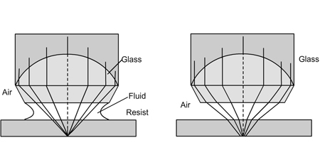
Fig 2.20. Schematic of immersion lithography
The requirements of the fluid are that it must be compatible with the photo resist and the lens and that it should not absorb the light used (< 5% absorption). High purity water satisfies these requirements. Its refractive index is 1.47 and it can be doped with sulfates or phosphates to increase the refractive index slightly. Commercially, water is continuously circulated between the wafer and the lens, and is maintained at a constant temperature since the refractive index can change with temperature. Care must be taken to ensure that it is particle free and bubble free, that it is removed after exposure, and that leaching from the photo resist is minimal.
Summary: To summarize, in the lithographic section in the manufacturing line, depth of focus is an important parameter for the production and this can be improved by CMP. Alignment is another important parameter and alignment masks are used for aligning the current level to the previous level. One should also be aware of the issue of partial field and be able to optimize the location of fields to obtain the maximum number of good chips. Immersion lithography can extend the use of current light sources by one generation. EUV lithography seems to be an emerging technique which may be used in the industry in the near future while X-ray lithography is still in research stage now. We will see the details of the deposition techniques in the next chapter. |