Now, in ideal case, there will not be any dust present and the lithography (exposure and developing) followed by etching will give the required structure. However, if dust particle falls on the mask, then a problem may arise. If the dust particle falls on the area which is already blocking the light, then it will continue to block the light and there will not be any issue. However if it falls in the transparent area, then the following scenario will arise in positive and negative resist cases.
If the particle is small, then it will block the light in a small area. In positive resist case, the structure, after developing will have small pillar like structures as shown in Fig. 2.6. Usually these pillars will not be stable and hence will fall away during the developing process. But if the particle is large, then they will protect the material below them, during the etch process. Thus, the structure will not be formed correctly if the particle is large.
In case of negative resist, even if the particle is small, it will result in a pinhole during developing stage and subsequently in the etching as shown in Fig. 2.6. Thus the structure will not be formed correctly for small as well as large dust particle. Hence, positive resist process is relatively more robust.
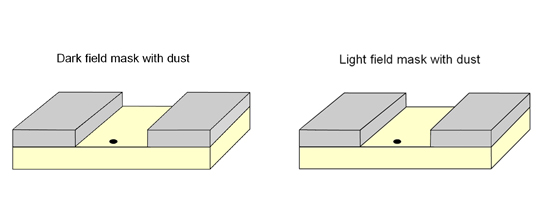
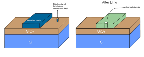
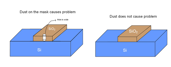
Fig 2.6 Dust falling on transparent areas.
Contact, Proximity and projection printing
We saw that using lens system the features on the mask were reduced to 4 or 5 times on the wafer. This is called projection printing (Fig 2.7c). A few decades back, two other types of masks were used. One is called contact printing(Fig 2.7a). In that case, the features on the mask will be the same size as the features on the wafer. The mask will be placed on top of the wafer, and it will be touching the photoresist. Hence the name contact printing is used. The disadvantage of this technique is that after a few wafers are processed, the photoresist will stick to the mask and the mask will have to be replaced. The second method was called proximity printing (Fig 2.7b). In this case, the mask will be held slightly above the photo resist. The features size on the mask was similar to the feature size on the wafer. Since the mask does not touch the wafer, the probability of mask damage is low. However, compared to projection printing, the mask still needs to be replaced occasionally. At present, only projection printing is used.
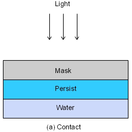
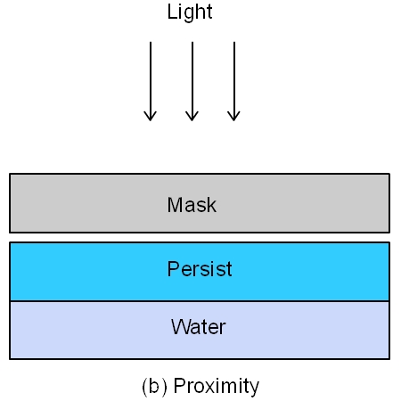
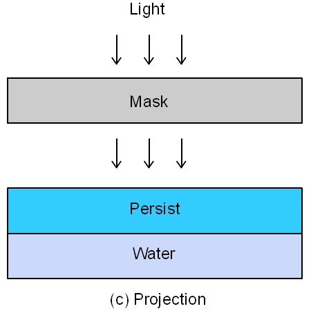
Figure 2.7 Different types of lithography
Although we have shown only one lens in the schematics here (Figure 2.5 Stage 3), in practice, the litho tool is very complicated and it will have complex lens system, facilities to control the lamp power and facilities to move the wafer and the mask in a very fine level.
Stepper vs. Scanner:
We saw that the lithographic equipment is also called a stepper because it exposes one part of the wafer to the light, and then moves or steps to the next location and repeats the exposure. Recently, a more sophisticated technique called scanning is used (Fig. 2.8). In this, the exposure is not done in one shot. Instead, once the mask is positioned above the wafer, light is shone on only a part of the mask and the wafer. Then the wafer and the mask are moved, as shown in figure. This step is called scanning. When the entire mask is covered, the scanning is completed. Then the wafer is moved to the next step and the scanning continues. Thus, even though the equipment is called as scanner, it is actually a step-and-scan technique.
What is the need for scanning? Large lenses, free from aberrations, are extremely expensive. If only a stepper is used, then for a given mask size, a very large lens is needed. The diameter of the lens must be at least 1.4 times the size of the mask.
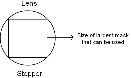
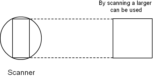
Figure 2.8: A scanner can handle a larger mask than a stepper (when both of them use the same sized lenses).
However, if scanning is available, then the task can be accomplished using a smaller lens. Consider the following example. During scanning, only a part of the mask is exposed. In this example, the entire ‘width’ of the mask is exposed at all the times, but only a small part of the ‘width’ is exposed. By moving the mask (and also the wafer), the entire mask can be covered while using a smaller lens. Even within this small lens, only a small part should be absolutely free from aberrations. Thus for a given mask a smaller lens can be used in step-and-scan systems. Alternatively, for a given lens, a larger mask can be used in a scanner while only a smaller mask can be used in a stepper.
Litho is a critical step in IC manufacturing. Many a times, the failure in the chip occurs because of some problem in litho. In other processes, there may be a way to compensate if any minor deviation occurs. For example, in deposition, if more material is deposited than necessary, then it is possible to adjust for it in the subsequent removal steps. We can remove a bit more than normal and we will be left with a good structure. In litho, if the problem is caught before etching, then we can completely remove all the resists and send
the wafer back for reprocessing. If there is mistake in the litho step, and if the wafer is etched, it is almost impossible to recover. If any dust falls on the wafer during the litho process, the defect will most likely lead to failure. Thus the litho area has to be maintained much more cleaner than all other locations in the fab.
|