Production Issues:
Next we will learn about four important topics in practical lithography. They are are 1. Resolution , 2. Alignment (misalignment) 3. Depth of focus and 4. Partial fields
1. Resolution: The resolution indicates the smallest feature or the spacing that can be produced in a manufacturing process. If we say that the resolution is 100 nm for a particular process ,we mean that we can make any structure which is 100 nm size or larger or we can produce structures with a spacing of 100 nm or more. It also means that we probably cannot make structures which are smaller in size (like 50 nanometer) or smaller in gap repeatedly in this process. It means that we do not have that ability.
What are the parameters that determine the resolution?
The resolution depends on the wavelength of the light used and another parameter called “Numerical Aperture”. The resolution also depends on the sophistication of machines, which is given by the parameter called “Raleigh constant”. For a given machine, the resolution basically depends on the wavelength and numerical aperture. Numerical aperture is a function of the diameter of the lens and the focal length of the lens and is given by  . .
Resolution is related to the wavelength (λ) and the numerical aperture (NA) as shown below.
 where k is the Raleigh constant. where k is the Raleigh constant.
So, to get better (i.e. smaller) resolution, we should decrease the wavelength of the light used and increase the numerical aperture. Can we keep reducing the wavelength and increasing the numerical aperture? The answer is no. This is because they affect another important parameter called depth of focus.
Depth of focus (also called depth of field) indicates how much variations one can accept in the planarity of the incoming wafer. For example if the incoming wafer is perfectly planer then it is easy to use the lithography process. Usually the incoming wafer will have some variation in the topography (some ups and downs). The lithography process should be able to print the patterns correctly even when there is poor planarity. This ability is quantified by the term “depth of field”. If the depth of field is large, it means that even if the incoming wafer has lot of variations in the height, the lithography process can tolerate it. So, ideally we want the best depth of field (i.e. large depth of field) and the best stability to resolve (i.e. smallest resolution). Unfortunately the depth of focus is related to the wavelength λ and the numerical aperture (NA).

So, if we make the resolution better by increasing the numerical aperture, we will lose depth of field lot more. Instead, if we make the resolution better by decreasing the wavelength, we will still lose some depth of field, but the loss is limited. Thus we cannot get large depth of field and still the smallest resolution. One has to make a compromise. We will see some more details about the depth of focus in the later section.
Even the wavelength of the light used cannot be arbitrarily decreased. Originally visible light was used in lithography process. Later ultraviolet (UV) light in the wavelength region was used. At present extreme UV (EUV) is being introduced for lithography. When the wavelength of the light is reduced, new problems arise.
When EUV is used, almost all the materials absorb the light and hence lens cannot be used. Reflective mirrors (concave mirrors) made of special materials must be used. When X-Rays are used, it penetrates almost all materials and hence cannot be easily used. Thus many litho processes use light of 193 nm wavelength, as of 2010.
Now given a wavelength, how can we improve the resolution? There are certain techniques called resolution enhancement technique (RET). We will consider three such techniques: one is optical proximity correction (OPC), second is anti reflective coating (ARC) and the third is phase shift mask (PSM).
A. OPC or Optical Proximity Correction : Proximity means ‘nearness’ or something in the vicinity. If we consider a metal line to be patterned in a particular location, the presence of a line nearby will affect the optical behavior. If we want to print two lines next to each other in one case, and print one line with no other line near it in another case, then there is some difference in the behavior of these two cases. Optical proximity correction is a method to adjust the layout so that the differences are accommodated and the printing occurs as planned. We will illustrate this with an example.
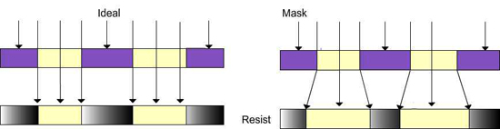
Figure 2.9 a and b. Diffraction effects
Figure 2.9a shows what should happen if diffraction effects are absent. This is marked as “ideal”. If we pass light through the mask, then the light should pass through the openings (i.e. transparent areas) and form an image on the wafer with exactly the same size and shape. In reality, the light will not form the parallel line. There is diffraction and hence the image on the wafer will be different compared to the image on the mask. This is shown in figure 2.9 b and is marked as “real”. Further, the image will also change more if there are neighboring lines. Thus, the presence or absence of neighboring lines makes a difference. Even if there is no other line nearby, the image will not be exactly the same as the one in the mask.
In the case of line without any neighbor, called isolated line or iso line, the diffraction effects may make the image bit smaller than planned. For example, if the mask contains 100 nm line, the image on the wafer may be only 90 nm. So, in order to print 100 nm line on the wafer, the mask can be made with 110 nm wide line. Please note that in this example, we are assuming that the mask is 1X mask and not the usual 4X mask. In case of a 4X mask, the explanation will be as follows. If we use 400 nm wide line in the mask, the ideal lithographic process will produce 100 nm wide image on the wafer. But the actual image may be 90 nm due to diffraction. Hence, to produce 100 nm image on the wafer, the mask may be made with 440 nm wide line. This method is called biasing and is one part of OPC. This is shown in figure 2.10 a and b. Figure 2.10 a, on the left side, is the layout before OPC and the figure 2.10 b, on the right side, is the layout after OPC. Notice the increase in size of some of the lines. Also notice that the left most line, which is already large, is not altered. Thus, not all the lines are altered by OPC.
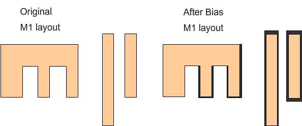
Figure 2.10 a and b. Biasing in layout
But we cannot just make all the lines larger and expect that everything will print correctly. A few more modifications are necessary. Depending on the method used to make the corrections, OPC can be classified as “rule based” or “model based”. Rule based OPC is somewhat empirical. For example, one rule may say that “If there are two lines separated by 200 nm, then increase the width by 10 nm. If they are separated by 300 nm, increase the width by 5 nm” etc. This is relatively simple and is reasonably effective. However, when one tries to make very complicated chips, this method is not very effective.
“Model based OPC” actually models how the light will travel and how diffraction will alter the image, over the entire mask .It is very computationally intensive. It can run on very powerful computers for many days for a single layer of mask. But if the modeling is done correctly, then the results are better than what one would obtain from rule based OPC.
A few examples of the changes made by OPC are shown in the figures 2.11a and 2.11b. Note that the width is increased a little and the line-end is extended a bit more.
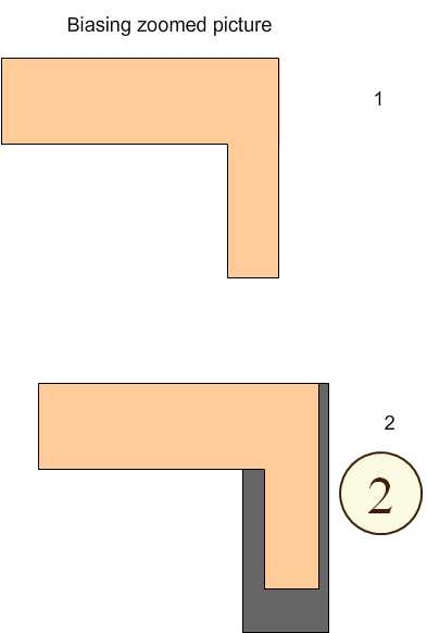
Figure 2.11 a and b. Example structures in layout (a) before OPC and (b) after OPC
The figure 2.12 a and b show a T shaped structure before and after OPC respectively. If one actually makes a mask with the T shaped structure without OPC, then the structure on the wafer will appear somewhat like the figure 2.12 c. i.e. it will cause “necking” or reduction in the neck of the T junction
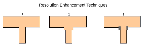
Figure 2.12 a, b and c. T junction in layout (a) before OPC, (b) after OPC and (c) result of printing on wafer, without doing OPC in the layout.
In order to ensure that a real T structure is obtained on the wafer, one needs to add little bit of squares near the T junction, as shown in fig 2.12 b. Sometimes these are referred to as “dog ears”. Thus we add dog-ears to the T junction so that it will actually print correctly on the wafer. Generally one needs to increase or decrease the width and add the dog ears. Thus, fig 2.13 a shows the ideal pattern that we want on the wafer on the left side and the figure 2.13 b on the right shows the layout after biasing and adding dog-ears, so that we will finally get the correct pattern on the wafer.
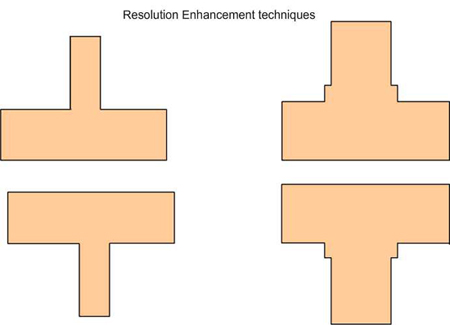
Figure 2.13 a and b. Adjacent T junctions in the layout (a) before OPC and (b) after OPC
One point that we need to remember is that increase in the width is not the same as enlarging the layout. Here when the width is increased, the space gets reduced.
The above illustrations are simplified version of the OPC process so that one can understand OPC. If one looks at the real mask before and after OPC, there will be a lot more changes. However, the basics are what we have seen here. One can search in the internet (for example in the web sites of companies like IBM or Intel) in order to gain some idea of what a mask looks like before and after OPC.
In the lithography process, the presence of one line will affect the printing of another line, if the distance between the lines is within one micron. If the distance is more than one micron, the presence or absence of a line will not make any difference. That is the effect is felt only up to one micron in lithography process, whereas if one looks at few other processes, the effect can be felt even further. For example, in a process called chemical mechanical planarization, the length scale where one feature affects the process of another, can be as high as mm. In these cases, the layout is again altered to account for these non-idealities. Techniques such as slotting and introducing dummy features are used to account for non-idealities in CMP. We will see those details in the “removal techniques” chapter.
|