Once the mask is made, it is used in the photolithography tool. Sometimes the tool is also called as “litho”. It is roughly 12 ft long, 12 ft wide and 8 ft tall. Here, an explanation is of order. If we say ‘car’, it can mean a very small car or a very large car. Similarly all the tools in IC manufacturing come in different sizes. Here we mention the size to give some rough idea. We do not mean that all the lithography tools will be exactly of the size mentioned here.
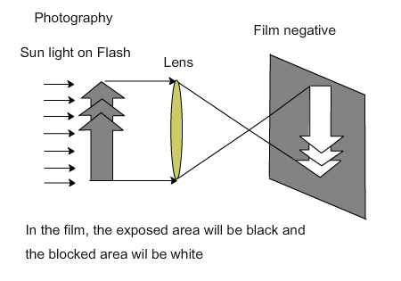
In litho tool, only one wafer is processed at a time. Its principle is very similar to taking photo using conventional cameras with film. When a camera film is used, first the film has to be inserted into the camera. Next the shutter is opened for a short time, and wherever the light falls on the film, some chemical reaction occurs. In the places where light doesn’t fall, no chemical reaction occurs. (Figure 2.3a)
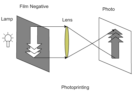
Figure 2.3 a. Creating a photographic negative Figure 2.3 b. Obtaining prints from a negative
After the photo is taken, the film has to be developed and it has to be done in a dark room. Although it is called as dark room, yellow colored lights are used inside to enable normal activities of the engineers and technician. This is because the photo resist used is not sensitive to yellow light, but light from other sources will cause chemical reactions in the film and alter the image. In a black and white film, wherever light has fallen, the film will be dark and wherever light is blocked, the film will be transparent or white. So, it is called a negative. Using a negative, we can make many copies of the photo. For that, a paper with light sensitive coating is needed. When we place the negative on top of the paper and shine light, the areas which are black will block the light and the transparent areas will allow the light (Figure 2.3 b). This light will cause reactions on the chemical coating on the paper. After this, the light sensitive paper is washed or developed in a suitable chemical solution and the photo will be ready.
To create larger or small photos from a negative, the light is passed through a lens. Then we can obtain a larger or smaller photo from the same negative. Likewise, the mask is used as negative in the IC manufacturing. Instead of paper, we use chemical coated silicon wafers. The chemical will be sensitive to light. Typically, the features or shapes on the mask will be four or five times larger than that on the wafer. The features are ‘shrunk’ on the wafer using a lens system. After the wafers are exposed to light in the litho tool with mask, the wafers are usually sent for ‘etching’. This is the summary of photolithography process. We will see the details below.
Why are the masks four or fives times larger than the image on the wafer? It is easier to make larger features on the mask. With this mask, all the layout features will shrink in size on the wafer. Any irregularities in the mask or any dust particle falling on the mask will also be shrunk and hence the image will be affected less.
Lithography process details:
Once the masks are ready, the wafer will be coated with a chemical called photo resist, sometimes called “resist”. The resist is sensitive to light. The resist will be dissolved in a solvent and poured over a spinning wafer. Due to the rotation of the wafer, the solution will spread uniformly over the wafer (Figure 2.4- Stage 1).
Figure 2.4 Lithographic process
After some solution is poured, the wafer will be made to spin at high speed (Figure 2.4- Stage 2). The solution will spread very thin and if the wafer is heated at this time, the solvent will evaporate. The resist will form a film on top of the wafer. This process is called soft baking. All these operations would be conducted in a dark room because light from any source will cause chemical reaction of the photo resist and will alter the patterns.
After this, the wafer and mask are brought into alignment. The lens system will be adjusted so that the focus is correct. Then light of particular wavelength will be made to fall on the wafer, through the mask, for a short time. Typically, the exposure is for a second. Wherever the light has fallen, the chemical reaction would have taken place (Animation 2.4 stage 3 and stage 4). Note that the image on the wafer is smaller than the image on the mask.
A mask will expose only a small area. The area may be about 5 cm x 5 cm. So, the whole wafer cannot be exposed in one shot. The wafer must be moved to the next location (e.g. 5 cm), and then the process of alignment, focus and exposure must be repeated (Figure 2.4 Stage 5). This procedure will continue until the entire wafer is exposed. Since it is done by moving the wafer in steps, the litho tool is also called “stepper”. After the whole wafer is exposed, it is sent for developing. The wafers are dipped in suitable solutions. Wherever the light has fallen, a chemical reaction would have occurred. Those areas will be dissolved in the developing solution. The areas where light did not fall will not dissolve (Figure 2.4 Stage 6)
If the wafer is heated now, the resist will harden a bit. This process is called hard baking (Figure 2.4 Stage 6). After baking, the resist will not move or show much flexibility. The litho process ends here.
Let us assume that the wafer is sent for etching after this. Here, the wafer may be dipped in a corrosive solution (wet etching) or corrosive gases may be passed on the wafer surface (dry etching). The areas protected by photo resist will not be corroded, while the areas left open will corrode or etch (Figure 2.4 Stage 7).
After etching for a certain time, the wafer will be cleaned. Then it will be dipped in a different solution, which is capable of removing the hardened photo resist (Figure 2.4 Stage 8)
Similarly, in each level, whenever a material has to be removed in certain areas, photolithography is used. Making a normal IC will need more than 30 masks.
Positive and negative resists:
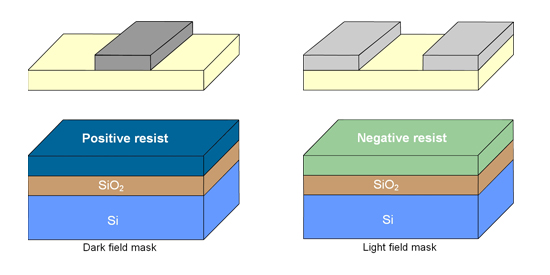
The commonly used resists fall under the category of positive resists. Here, the regions exposed to light dissolve in the next stage of litho process. Thus, the pattern formed on wafer is the same as the pattern present on the mask. A few decades back, another type of resist called negative resist was used. In those resists, the regions exposed to the light will not dissolve but the regions where the light is blocked by the mask will dissolve. Typical negative photoresists are polymers with photo sensitive chemicals. In presence of light, the polymers will cross link and will be less soluble. In case of positive resists, a photo active compound which is normally not soluble in the developer is used. In presence of light, the compound changes its structure and becomes soluble.
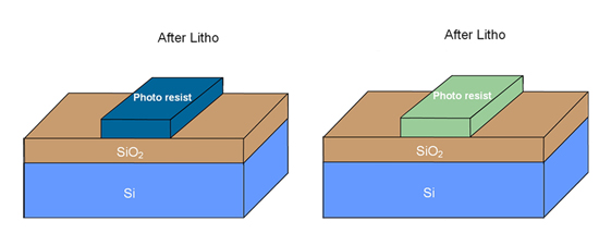
One of the advantages of the positive resist over negative resist is that the process is relatively less sensitive to dust particles. Consider the following example. If we want to etch the material and obtain a particular structure, the mask may be made as shown in the figure 2.5. For a process using a negative resist, to get the same feature on the wafer, the mask will be different, as shown in figure 2.5. The masks are called as dark field mask and as light field mask respectively. It is possible to use either dark field mask or a light field mask with positive photo resist or negative photo resist. However, in industry, usually dark field masks are used now and with positive photo resists.
FIGURE 2.5 Litho for positive and negative resists.