Large MOS transistors are susceptible to the latch-up effect. In the chip substrate, at the junctions of the p and n material, parasitic pnp and npn bipolar transistors are formed as in the following cross-sectional view shown in Figure 33.51
Fig 33.51: Latch-Up
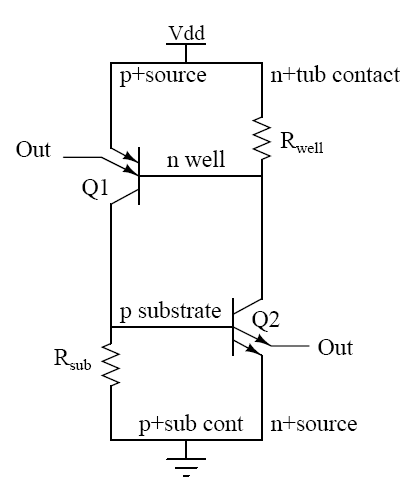
These bipolar transistors form a silicon-controlled rectifier (SRC) with positive feedback as in the following circuit model shown in Figure 33.52
Fig 33.52: SRC With Positive Feedback
The final result of the latch-up is the formation of a short-circuit (a low impedance path) between VDD and GND which results in the destruction of the MOS transistor.