ESD damage is usually caused by poor handling procedures. ESD is especially severe in low humidity environments. Electrostatic discharge is a pervasive reliability concern in VLSI circuits. It is a short duration (<200ns) high current (>1A) event that causes irreparable damage. The most common manifestation is the human body ESD event, where a charge of about 0.6uC can be induced on a body capacitance of 100pF, leading to electrostatic potentials of 4KV or greater.
Whenever body comes in contact with plastic or other insulating material, static charge is generated. It can be a very small charge, as low as nano Coulombs, but it can cause potential damage to MOS devices, as voltages are pretty high.
We know that
Q = CV
V = Q/C
V = It/C
Let us consider a modest 1pF capacitor, in which, this 1nC charge is put (can be through a 100uA current for a millisec). This results in
breakdown voltage is volts/meter. If gate oxide is about 0.1um thick, say;
Maximum allowable voltage is .
This can easily be generated by walking across a carpet!! A human touch can produce instanteous voltages of 20,000 volts!
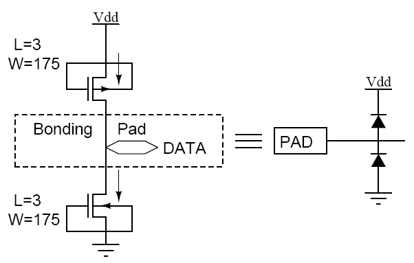
A typical solution of the ESD protection problem is to use clamping diodes implemented using MOS transistors with gates tied up to either GND for nMOS transistors, or to VDD for pMOS transistors as shown in Figure 33.21. For normal range of input voltages these transistors are in the OFF state. If the input voltage builds up above (or below) a certain level, one of the transistors starts to conduct clamping the input voltage at the same level.
Fig 33.21: Clamping Transistors
These clamping transistors are very big structures consisting of a number of transistors connected in parallel, and are able to sustain significant current. The thick field NMOS used design is not suitable for deep submicron processes, and the thin field oxide NMOS presents oxide breakdown problems while interfacing between blocks with high power supply voltages.
Scaling of VLSI devices have reduced the dimensions of all structures used in ICs and this has increased their susceptibility to ESD damage. Hence ESD protection issues are becoming increasingly important for deep submicron technologies. The gate oxide thicknesses are approaching the tunneling regime of around 35 Angstroms. From an ESD perspective, the important issue is whether the oxide breakdown is reached before the protection devices are able to turn on and protect them!

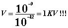
 breakdown voltage is
 volts/meter. If gate oxide is about 0.1um thick, say;
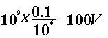 .