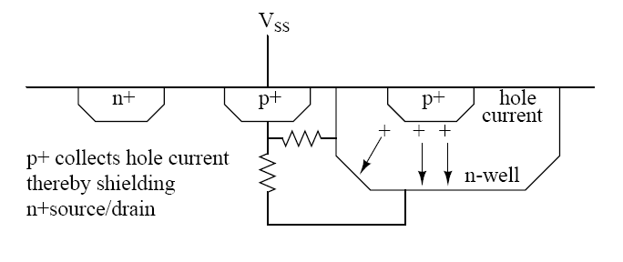
The following techniques can be used to prevent latch-up:
Use p+ guard rings to ground around nMOS transistors and n+ guard rings connected to VDD around pMOS transistors to reduce Rwell and Rsub and to capture injected minority carriers before they reach the base of the parasitic BJTs
Place substrate and well contacts as close as possible to the source connections
Use minimum area p-wells (in case of twin-tub technology or n-type substrate) so that the p-well photocurrent can be minimized during transient pulses
Source diffusion regions of pMOS transistors should be placed so that they lie along equipotential lines when currents flow between VDD and p-wells. In some n-well I/O circuits, wells are eliminated by using only nMOS transistors.
Avoid the forward biasing of source/drain junctions so as not to inject high currents; the use of a lightly doped epitaxial layer on top of a heavily doped substrate has the effect of shunting lateral currents from the vertical transistor through the low-resistance substrate.
Layout n- and p-channel transistors such that all nMOS transistors are placed close to GND and pMOS transistors are placed close to VDD rails. Also maintain sufficient spacings between pMOS and nMOS transistors.