| |
| 33.3 Output Buffer |
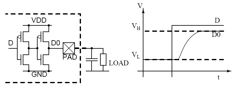
| The intra-chip buffer circuits are relatively well known. They are fast, and need only be as big as needed to drive their particular load capacitances. However, in the inter-chip buffer design case, there are some very important limitations. First, these buffers must be able to drive large capacitive loads, as they are driving off-chip signals, which means driving I/O pads, parasitic board capacitances, and capacitances on other chips. Adding a few picofarads of capacitance at the output node is really inconsequential, and shouldnt significantly degrade the propagation delay through this structure. So, the O/P load for worst case design is considered to be 50 times normal load, approximately 50pF. The simplest driver for the output pad consists of a pair of inverters with large transistors in addition to the standard ESD protection circuitry. The driver must be able to supply enough current (must have enough driving capability) to achieve satisfactory rise and fall times (tr, tf) for a given capacitive load. In addition the driver must meet any required DC characteristics regarding the levels of output voltages for a given load type, viz. CMOS or TTL. |
| |
|
Fig 33.31: Output Buffer |
| |
| Design method is same as we have already discussed in previous lectures. Optimum number of stages are found for a load capacitance assumed a-priori. Logical effort method can be used to decide sizing. |
| |
| Second, the voltage across any oxide at any time should not be greater than the supply voltage, which ensures oxide reliability; most process design engineers will not guarantee oxide reliability for oxide voltages greater than the chip VDD. If a low voltage chip is tied to a bus which connects several chips, some with higher supply voltages, then the Input buffer must be designed such that there is no chance of a problem with the oxide. |
| |
|
| |
| |
| |
| |
| |
| |
| |
| |
| |
| |
| |
| |
| |
| |
|