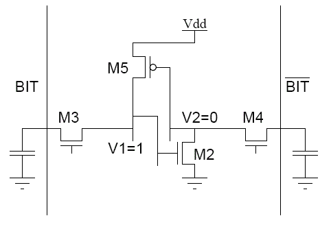
Consider the write '0' operation assuming that logic '1' is stored in the SRAM cell initially. Figure 28.51 shows the voltage levels in the CMOS SRAM cell at the beginning of the data write operation. The transistors M1 and M6 are turned off, while M2 and M5 are operating in the linear mode. Thus the internal node voltage and before the access transistors are turned on. The column voltage is forced to '0' by the write circuitry. Once M3 and M4 are turned on, we expect the nodel voltage to remain below the threshold voltage of M1, since M2 and M4 are designed according to Eq. 28.1.
Fig 28.51: SRAM start of write '0'
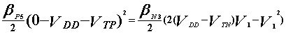
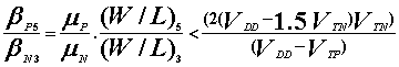
The voltage at node 2 would not be sufficient to turn on M1. To change the stored information, i.e., to force and , the node voltage must be reduced below the threshold voltage of M2, so that M2 turns off. When the transistor M3 operates in linear region while M5 operates in saturation region. Equating their current equations we get