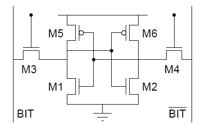
A low power SRAM cell may be designed by using cross-coupled CMOS inverters. The most important advantage of this circuit topology is that the static power dissipation is very small; essentially, it is limited by small leakage current. Other advantages of this design are high noise immunity due to larger noise margins, and the ability to operate at lower power supply voltage. The major disadvantage of this topology is larger cell size. The circuit structure of the full CMOS static RAM cell is shown in Figure 28.12. The memory cell consists of simple CMOS inverters connected back to back, and two access transistors. The access transistors are turned on whenever a word line is activated for read or write operation, connecting the cell to the complementary bit line columns. |