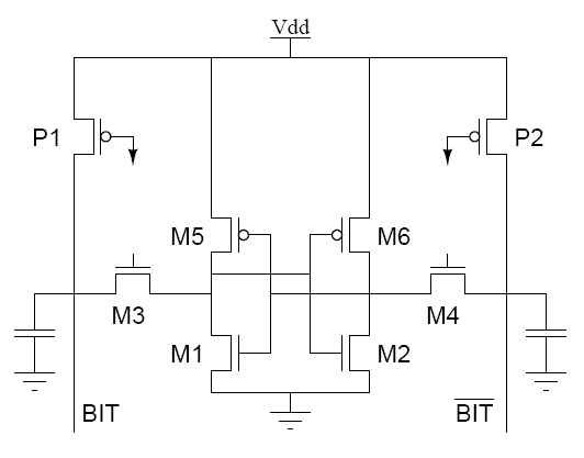
To detemine W/L ratios of the transistors, a number of design criteria must be taken into consideration. The two basic requirements, which dictate W/L ratios, are that the data read operation should not destroy the stored information in the cell. The cell should allow stored information modification during write operation. In order to consider operations of SRAM, we have to take into account, the relatively large parasitic column capacitance and and column pull-up transistors as shown in Figure 28.31.
Fig 28.31: CMOS SRAM cell with precharge transistors
When none of the word lines is selected, the pass transistors M3 and M4 are turned off and the data is retained in all memory cells. The column capacitances are charged by the pull-up transistors P1 and P2. The voltages across the column capacitors reach .