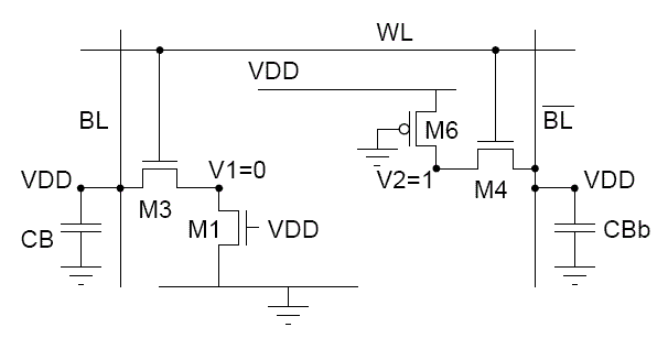
Consider a data read operation, shown in Figure 28.41, assuming that logic '0' is stored in the cell. The transistors M2 and M5 are turned off, while the transistors M1 and M6 operate in linear mode. Thus internal node voltages are and before the cell access transistors are turned on. The active transistors at the beginning of data read operation are shown in Figure 28.41.
Fig 28.41: Read Operation
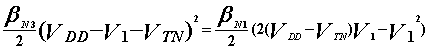
After the pass transistors M3 and M4 are turned on by the row selection circuitry, the voltage of will not change any significant variation since no current flows through M4. On the other hand M1 and M3 will conduct a nonzero current and the voltage level of will begin to drop slightly. The node voltage will increase from its initial value of '0'V. The node voltage may exceedthe threshold voltage of M2 during this process, forcing an unintended change of the stored state. Therefore voltage must not exceed the threshold voltage of M2, so the transistor M2 remains turned off during read phase, i.e.,
(Eq 28.1)
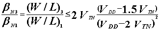
The transistor M3 is in saturation whereas M1 is linear, equating the current equations we get