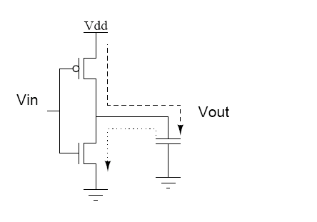
During switching, either from '0' to '1' or, alternatively, from '1' to '0', both n- and p-transistors are on for a short period of time. This results in a short current pulse from to . Current is also required to charge and discharge the output capacitive load. This latter term is usually the dominant term. The current pulse from to results in a 'short-circuit' dissipation that is dependent on the input rise/fall time, the load capacitance and the gate design.
Fig 26.61: Power dissipation due to charging/discharging of capacitor
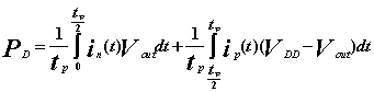
The dynamic dissipation can be modeled by assuming that the rise and fall time of the step input is much less than the repetition period. The average dynamic power, , dissipated during switching for a square-wave input, , having a repetition frequency of , is given by
(Eq 26.8)
where
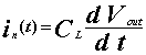
= n-device transient current
= p-device transient current
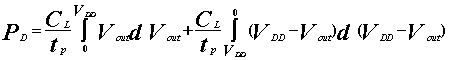
For a step input and with
(Eq 26.9)
(Eq 26.10)
with ,
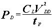
resulting in
(Eq 26.11)
Thus for a repetitive step input the average power that is dissipated is proportional to the energy required to charge and discharge the circuit capacitance. The important factor to be noted here is that Eq 26.11 shows power to be proportional to switching frequency but independent of device parameters.
The power dissipation also depends on the switching activity, denoted by, .
 , is given by