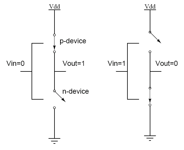
Consider the complementary CMOS gate, shown in Figure 26.51
Fig 26.51: CMOS inverter model for static power dissipation evaluation
When input = '0', the associated n-device is off and the p-device is on. The output voltage is or logic '1'. When the input = '1', the associated n-device is on and the p-device turns off. The output voltage is '0' volts or . It can be seen that one of the transistors is always off when the gate is in either of these logic states. Since no current flows into the gate terminal, and there is no DC current path from to , the resultant quiescent (steady-state) current, and hence power , is zero.
However, there is some small static dissipation due to reverse bias leakage between diffusion regions and the substrate. In addition, subthreshold conduction can contribute to the static dissipation. A simple model that describes the parasitic diodes for a CMOS inverter should be looked at in order to have an understanding of the leakage involved in the device. The source-drain diffusions and the n-well diffusion form parasitic diodes. In the model, a parasitic diode exists between n-well and the substrate. Since parasitic diodes are reverse biased, only their leakage current contributes to static power dissipation. The leakage current is described by the diode equation:
(Eq 26.6)
where,
= reverse saturation current
V = diode voltage
q = electronic charge
k = Boltzmann's constant
T = temperature
The static power dissipation is the product of the device leakage current and the supply voltage: