SEM: ELECTRON BEAM INDUCED CURRENT
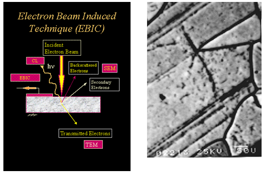
Figure 17.07: Schematic of EBIC set up and image showing electronically active defects in solar-grade Si. [10].
Electron Beam Induced Current (EBIC) mode is applicable to semiconductor devices. When the primary electrons strike the surface, electron-hole pairs are generated and the resulting current is collected to modulate the intensity of the CRT image.
This technique is useful in spatially locating subsurface defects and failure sites within a junction region.
Ref.[10]. http://www.tf.uni-kiel.de/matwis/amat/def_en/kap_6/illustr/i6_1_7.html.