Certain techniques are used to ensure that the deposition is uniform. The wafer can be rotated slowly. If the wafer is heated, then the deposited layer can soften and move and also stick well.
What is the advantage of using argon to hit the target and deposit the material on the wafer? Why not just use evaporation?
Materials such as tungsten have very high melting point (3422 oC) and boiling points (5555 oC). It will be very difficult and energy intensive to deposit tungsten by evaporation. Besides, if an alloy has to be deposited, the composition of the vapor will not be the same as that of alloy. Materials with low boiling point will tend to evaporate early. However, in PVD, since the material is removed by the bombardment of argon ions, the operation can be conducted at relatively low temperature. Alloys can be deposited with out difficulty.
Why do we have to use argon? Argon is an inert gas which will not react with the target or the wafer surface. If we use oxygen or nitrogen instead, they may react with the target and or the wafer surface. We can use other inert gases such as helium or neon. However, it is more difficult to ionize helium or neon. They are also more expensive than argon. Hence argon is used for sputtering.
PVD can be used for depositing tungsten, titanium, tantalum, copper, Titanium nitride and tantalum nitride. Currently titanium and tantalum metals and their nitrides are deposited using PVD. Tungsten is deposited using chemical vapor deposition or CVD. A thin layer of copper, called seed layer, is deposited using PVD while the remaining copper is deposited using electrochemical deposition.
RF sputtering: All the materials we saw above are electrical conductors. PVD can be modified so that insulators such as silicon dioxide or silicon nitride can also be deposited.
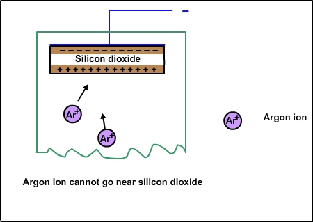
Figure 3.6. Problem in using insulator as target in PVD
What is the problem in using regular PVD for depositing an insulator like silicon dioxide?
Let us look into the figure 3.6. This explains the problem in using the normal PVD chamber to deposit and insulator like silicon dioxide. In the beginning, argon ions will come and hit the silicon dioxide and some of the silicon dioxide will be removed from there and deposited on the wafer. But, the argon will get stuck on the silicon dioxide. Since it is an insulator, the charge will not be removed. The silicon dioxide will acquire a positive charge. The backside of the glass will have negative charge, but there will not be any electrical conduction. Very soon, the entire surface will be positively charged and argon ions, which are also positively charged, cannot approach the glass. The argon ions will not be able to hit the target and deposit the target material on the wafer. If we were using a metal, then the positive charge will be neutralized because the metal will conduct the electron from the backside to the plasma side.
In order to deposit the insulator by PVD, electrons must be supplied to the surface of the insulator on a regular basis. This is achieved by using radio frequency (RF) AC voltage. This is sometimes called as RF sputtering.
How does the RF PVD function? The chamber, which uses RF sputtering, looks very similar to the one with normal sputtering, but the voltage applied will be different in this case. This is explained in the schematics shown in figure 3.7 and 3.8. If we take an AC voltage and add it to a DC voltage, then we will get a combined voltage as shown in this figure. If we apply only a pure AC voltage, then 50% of the time the wafer will be positive and 50% of the time the target will be positive. But when we apply the combined DC plus AC voltage, the wafer will be positive 75% of the time and the target will be negative for most of the time. For a short time, the target will be positive and the wafer will be negative.
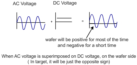
Figure 3.7. RF sputtering. Superimposing AC on DC
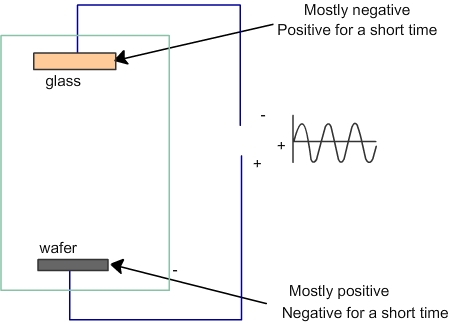
Figure 3.8. Schematic of RF sputtering chamber
What is the use of this? What will happen when this RF AC voltage is applied along with the DC? When the target is mostly negative, argon ions will come and hit it. Some of the electrons will go and hit the wafer. The glass will be removed by the argon ion and they will go and deposit on the wafer. For a short time, the electrode will be positive near the target; that time the electrons in the plasma will be attracted to the target. They will hit the target. The target has argon ions and the electrons will go and neutralize the argon ions, as shown in Fig. 3.9. Hence, the target will become neutral. Essentially, the electrons are supplied to the target surface from the plasma side and not from the electrical contact at the back.
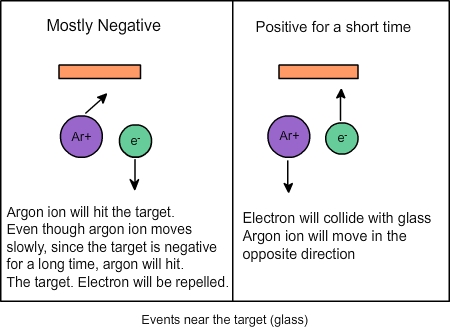
Figure 3.9. RF sputtering. Events near the target
Now will the argon ions go and hit the wafer in the same time? Because argon is much more heavier than electron, and because the duration is very short, it will not hit the wafer that much. Since the electrons are very light (low mass), they will not cause any damage and no atom will be taken out because of the electrons.

Figure 3.10 RF sputtering. Events near the wafer
We saw that argon ions will not hit the wafer because it’s for a shorter duration. Even if they hit, they will hit with less force and few hits will occur. In the beginning, in fact, the wafer will be made negative and the target will be made positive. Because of this, the argon will hit the wafer a little, and remove some material and make it rough. This actually facilitates good deposition of the material in the later stages. The initial roughening of the wafer will also help in cleaning any of the contaminant deposited on the material before this process.
Now the AC has to be applied at a very high frequency. That is why it is called RF or radio frequency. Now almost all of the sputtering equipment are RF sputtering equipment.
|