APCVD and LPCVD:
There is also another CVD method run at normal pressure. It is called atmospheric pressured CVD or AP-CVD. Here the temperature is relatively higher, in the range of 600 to 800 oC. In this method, a thick film can be formed quickly. However, there is risk of generating many dust particles and the film quality will be poorer. This method is used only in a few select cases.
Mass transfer control vs Reaction control: The following steps occur during CVD. First the reactant molecules diffuse through the boundary layer near gas-solid interface. Next the adsorb on the surface. In the third step, they diffuse on the surface. In the fourth step, they react with each other and the solid product is formed. Any gaseous byproduct formed may be adsorbed on the surface. Next, they desorb and diffuse outwards into the gas stream and get carried away.
When high temperatures are used, the reaction rate is very high and the rate of diffusion of the reactants through the boundary later decides the film growth rate. On the other hand, when the temperatures are lower, the mass transfer rate will decrease a bit, but the reaction rate will decrease a lot, and the surface reaction rate will decide the film growh rate. A plot of film growth rate vs inverse of temperature will appear as shown below.
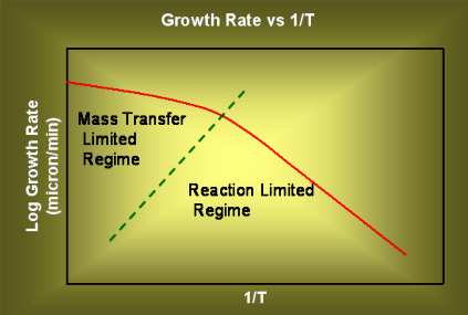
Figure 3.19. A qualitative plot of growth rate (in log scale) vs inverse of temperature.
The two different zones where diffusion is rate limiting and kinetics are rate limiting are marked.
APCVD is usually operated in high temperature regime, i.e. the film growth rate is diffusion controlled or mass transfer controlled. LPCVD is usually operated in relatively low temperatures and is reaction rate controlled.
We saw that sometimes the temperature has to be raised to anywhere between 150 to 1000 oC. For lower temperatures, normal heaters may be used. For high temperatures, heating lamps are used. The lamps enable us to start and stop the heating very quickly. This in turn results in good control of the deposition process.
Of late, organic gases containing metal atoms or ions are used in CVD. These are called metal-organic or MO-CVD. Based on a process that is similar to CVD, it is possible to create films of certain materials with exactly one atom thickness! This is called atomic layer deposition (ALD).
Atomic Layer Deposition: ALD can be thought of as a CVD technique with precise flow control. Consider a reaction between water vapor and trimethyl aluminum (TMA) to produce alumina (Al2O3) layer. The overall reaction is

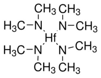
If both reactants are supplied to the chamber containing wafer, alumina layer will form on the wafer, but the thickness will not be easy to control. However, in ALD, first only water vapor is sent to the chamber. A monolayer of water will chemisorb onto the wafer. Then the chamber is evacuated and all the water vapor present, except the adsorbed molecules, will be removed. Next, a pulse of TMA is introduced in the chamber. Now, the TMA will react with limited water molecules present on the wafer and produce exactly one layer of alumina. The chamber is evacuated again and the water vapor and TMA are sent in sequence to grow the exact number of alumina layers required. At present, ALD is used for growing gate oxides in the advanced chips. Instead of SiO2, other materials such as HfO2 (hafnium oxide) are used as gate oxide in these chips and ALD offers the control necessary to deposit thin layers. The reaction between tetrakis dimethyl amido hafnium (structure given below) and water or ozone results in hafnium oxide.
Similarly, tetrakis dimethyl amido zirconium and water can be used as two reactants to obtain zirconia (zirconium oxide) in ALD.
Molecular beam epitaxy: Another technique in research stage is called molecular beam epitaxy (MBE). This is done in very high vacuum (10-8 Pa). The material to be deposited is heated and the molecules (or atoms) will evaporate. The wafer is kept at a lower temperature. Due to the high vacuum, the molecules will have a long mean free path and will not interact with one another. They will deposit on the wafer and due to the slow growth rate, it is possible to get single crystal growth using MBE. The main disadvantage of MBE is that it is a very slow process and hence is not yet suitable for implementation in semiconductor industry.
Copper deposited by PVD or CVD method has slightly higher resistance than the film deposited using electrochemical methods. Hence electrochemical deposition (ECD) is used for coating the wafer with copper.
Electrochemical deposition (ECD):
Copper is used as interconnect material in the ICs. Copper can be deposited by PVD or CVD. However, the copper deposited by ECD has a lower resistivity and a better fill characteristic. The basic principle of electrochemical deposition is very simple. One can even try it at home. You can take two normal batteries and stack one on top of another and get a 3 volt battery combination. Two metal plates (e.g. key or shaving blade) should be connected to the positive and negative end by wires. In a glass beaker, some water and copper sulfate should be taken. If the metal plates are dipped inside the solution, without touching each other and then the connected to the batteries, then copper will deposit onto the metal connected to the negative terminal and oxygen will evolve from the metal connected to the positive terminal. In this system, the metal connected to the negative terminal is called cathode and the metal connected to the positive terminal is called anode. Using the same principle, gold or silver is also coated on inexpensive ornaments.
We have to remember that silicon is a semiconductor and the wafer must be made conductive for electrochemical deposition. Therefore, a thin layer of copper is deposited on the wafer using PVD or CVD first. This is called seed layer. Then the wafer is kept in a tank containing copper sulfate solution. The negative terminal of a voltage controlling system is connected to the wafer while the positive terminal will be connected to a copper block. When copper is deposited on the wafer, the copper content of the solution will decrease. If we use copper block as anode, then copper will dissolve from it and the solution will have a uniform and constant copper content. By controlling the temperature of the bath and the voltage applied, the thickness of the copper deposited can be controlled.
Apart from copper sulfate, a few other chemicals are usually added to the bath. This enables the deposited film to have good quality, without voids. Fig 3.20 shows a poor quality deposit and the good quality deposit. Certain large organic chemicals, called macromolecules, are added to the bath to obtain a leveled surface. These molecules tend to adsorb on the surface and suppress the deposition rates. They are more likely to adsorb on the flat surface and less likely to adsorb inside trenches and holes. Thus, they reduce the deposition rate on the top surface, but do not affect the deposition rate inside the trench and holes significantly. These are called suppressors or levelers. Certain chemicals called accelerators are also added to the electrochemical bath. They improve the deposition rate. They compete with suppressors in adsorbing to the surface and tend to adsorb more inside the trenches and holes. They also lead to less surface roughness and more uniform grain size of the deposit. They are sometimes called as brighteners. The addition of suppressor and brighteners in appropriate concentration makes the ‘bottom up’ fill possible in electrochemical deposition of copper. Note that the mechanism of action of suppressors and brighteners are not always supported by experimental evidence and in many cases remain as hypothesis. However since they result in good quality film, they are used commercially.
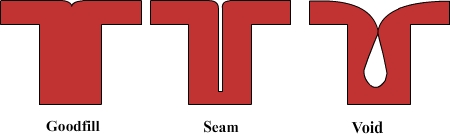
FIGURE 3.20. Examples of poor quality deposits and good quality deposits
While PVD or CVD can be used to coat copper on the wafer, it is used only for coating the seed layer. This is because superior quality copper is obtained by electrochemical deposition. For example, the electrical resistance of the copper obtained by electrochemical deposition is lower than that obtained by CVD or PVD. Another important property called electromigration-resistance, is more for electrochemically deposited copper. Electromigration is the tendency of the material to move with flow of current. If electromigration is high, then the wire will degrade soon and hence is not suitable. If electromigration resistance is high, then the material is considered as suitable. Thus, the ideal interconnect material should have low electrical resistance and high electromigration resistance. If the grain size of the deposited metal is large, it will tend to have better electromigration resistance. Since electrochemically deposited copper has large grain size and achieves low electrical resistance and high electromigration resistance, this method is used in semiconductor industry for depositing copper.
Spin on coating:
This method is used for depositing organic materials. The equipment is similar to the tool used in lithography for coating photo resist on to the wafer. First, the material to be deposited is dissolved in a solvent such as acetone or ethanol. Next, the wafer is kept on a platform and is rotated at about 500 rpm. While the wafer is spinning, the solution is poured on the wafer. Due to the rotation, the solution will spread on the wafer. Then the wafer is rotated at higher speed (about 5000 rpm). This controls the thickness of the solution. If the wafer is also heated, the solvent will evaporate, leaving the material on top of the wafer in the form of a film.
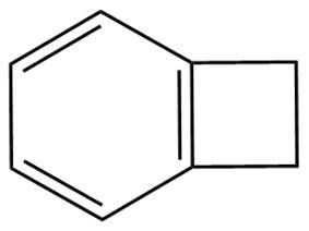
Traditionally silicon dioxide is used as the insulator between copper wires. Recently some materials called low-k materials, which have low dielectric constant, are used as insulators. Some examples of low-k materials are poly-tetrafluroethylene (PTFE, also called Teflon), benzo cyclobutene and polyimide (structure given below) This enables the chip to run faster and reduce the electrical current loss. Spin-on method is used to deposit the low-k materials.
 .jpg)
(a) (b)
Fig 3.21 Structure of (a) benzocyclobutene and (b) imide
In the next section, we will see the techniques used to remove excess materials, under the topic “removal methods”.
|