Collimated and Ionized Metal Plasma (IMP):
There are some more advanced techniques in the PVD. One is called collimated PVD. Another is called ionized metal plasma or IMP PVD.
During deposition, we want uniform deposition on the wafer. i.e. the deposited film thickness must be the same at the centre of the wafer, at the edge of the wafer and anywhere in-between.
If the target is very small compared to the wafer, it will look like a point source for the deposited material. In that case, the wafer centre will have higher deposition and the wafer edge will have lower deposition.
- One way to improve this is to increase the target size. If the target is large, then the deposition will be uniform. In that case, the target can be near the wafer and still we can get uniform deposition.
- On the other hand, we can pull the target away. If it is too far away, then most of the wafer will be more or less at the same distance from the target and hence, the deposition will be uniform. This is called “long throw”.
- Additionally, the wafers can be rotated during the process, and this also helps in obtaining uniform film thickness.
However if we increase the target distance, then the chamber will become very large and to evacuate the chamber and operate, one will spend correspondingly high energy. The goal of uniform deposition can be achieved by another method called collimated beam. A schematic is shown in the figure 3.11.
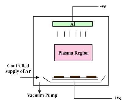
Figure 3.11 Collimated beam PVD
In this, a plate with holes is placed between the target and the wafers. The target atoms, which are coming towards the wafer, will have to come in straight line. Only then they will pass through the collimated plate. Otherwise, they will be stopped by the plate. This ensures that all of them are coming at similar angle and the film deposited will be uniform.
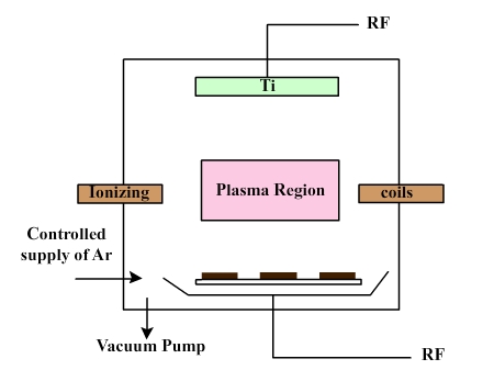
Figure 3.12, Ionized Metal Plasma (IMP) PVD
The most advanced method to obtain uniform thickness is called ionized metal plasma or IMP. A schematic of the IMP sputtering equipment is shown in figure 3.12. In this, the metal clusters that are coming towards the wafers are ionized using ionizing coils. Thus the titanium or aluminum metal atoms that are coming are ionized. They become charged and they will be attracted towards the wafer. Hence, even if they start at a different angle when they ejected out of the target, they will all move vertically towards the wafer because of the attractive forces. Since they are all coming at similar angles, the deposition will be uniform. The best quality of the film is obtained when IMP sputtering is used.
In the next section we will look into the second deposition technique, viz. CVD.
Chemical Vapor Deposition
In the PVD method described above, it is not easy to deposit a material on the side walls as shown in fig 3.13. This is especially true if the depth is very high and the opening si small. If the ratio of diameter (or width) to the depth, known as aspect ratio, is very high, PVD cannot give a good side wall coverage (Figure 3.14). However, CVD can be used to get a good side wall coverage (Figure 3.15).
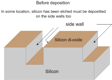
Figure 3.13. Schematic of wafer and sidewall before deposition
NV.jpg)
Figure 3.14. Illustration of a poorly deposited film
nv.jpg)
Figure 3.15 a . Illustration of a good film during deposition
NV.jpg)
Figure 3.15b. Illustration of a good film at the end of deposition
|