A large CVD chamber may be of 6 ft long and 3 ft diameter. In this, a material may be deposited on a lot (i.e. a batch) of 25 wafers. The CVD chamber will have pipes and automatic valves to create vacuum and to supply desired gases at controlled rates. The material to be deposited (e.g. tungsten) will be in the form of a compound, in the gaseous form. The CVD chamber will also have facilities to heat the wafers in a controlled fashion. A simple schematic of a CVD chamber is given in Figure 3.16
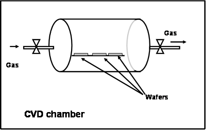
Figure 3.16. Schematic of a CVD chamber
Operation: First the wafers are kept in the chamber and the chamber is evacuated. Then the wafers will be heated to the desired temperature. Next the gases are supplied and they react only on the surface of the wafer and deposit the material. For example, let us assume that we want to deposit tungsten on the wafer. For this, a mixture of tungsten hexa fluoride, hydrogen and nitrogen (all in gaseous form) will be supplied to the chamber at low pressure. The temperature of the wafer would be maintained between 150 to 300 oC. In the CVD technology, the phrase “high temperature” refers to 800+ oC and low temperature may refer to “less than 400 oC”. Very low temperature may refer to room temperature.
In most of the CVD tools, all the chamber walls will be maintained at relatively lower temperature compared to the wafer. Only the wafers would be heated. WF6 and H2 will react only at high temperature. Hence the reaction will occur only on the wafer and not on the chamber walls. This type of CVD process is called low pressure CVD or LPCVD. Using this method many materials such as W, Ti, TiN, Cu, SiO2, Si3N4, Si etc can be deposited on wafer. The side wall coverage will also be good.
Some example reactions to deposit various materials are given below.
1. To deposit silicon
SiCl4 + 2 H2 → Si + 4 HCl
SiH4 → Si + 2H2
2. To deposit poly silicon
SiH4 → Si + 2H2
3. To deposit silicon di oxide
SiH4 + O2 → SiO2 + 2H2
SiH4 + 2N2O → SiO2 + 2N2 + 2H2
SiH2Cl2 + 2 N2O → SiO2 + 2N2 + 2HCl
4. To deposit Silicon nitride
3 SiCl2H2 + 4 NH2 → Si2N2 + 6H2+ 6 HCl
SiH2 + NH2 → SixNyHz+ H2 (some hydrogen is incorporated in the film)
5. To deposit Tungsten
WF2 + 3 Si → 2W + 3 SiF4
WF6 + 3 H2 → W + 6HF
There are certain disadvantages associated with the CVD process. Many of the gases used in CVD and highly corrosive and toxic. Hence good safety measures need to be taken. Also, the cost of the high purity chemicals is also high.
If the temperature and pressure are not controlled well, the reaction will occur in air itself and form tungsten (or whatever we are trying to deposit). These tungsten will appear like a dust and will fall on wafer. This dust particle will not stick well to the wafer and will degrade the deposited film quality.
The temperature cannot be raised arbitrarily during chip manufacturing. This is because a transistor is made with impurities doped in particular location. When the silicon wafer is heated, the dopants will move and the transistor will not function properly as shown in Figure 3.17 and Figure 3.18 . To avoid this, the wafer must not be heated. Then how do we deposit the material? Plasma comes to help here.

Figure 3.17 Schematic of a transistor at room temperature
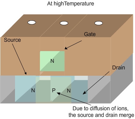
Figure 3.18. Schematic of a transistor at high temperature. Note that the diffusion causes merging of source and drain, leading to failure.
If the WF6 and other gases are passed while a high electric voltage is applied in the chamber, plasma will form. This is similar to creating plasma in PVD. Now the reaction will occur even at low temperature. This type of CVD is called Plasma Enhanced CVD or PE-CVD. In this method, high magnetic field can be applied to increase the density of plasma and improve the deposited film quality. This process is called High Denisty Plasma CVD or HDP-CVD.
We saw the materials such as silicon dioxide can be deposited using CVD. For example, Tetra Ethyl Oxy Silane (TEOS) can be heated to high temperature (or disintegrate in presence of plasma) and form silicon dioxide. Similarly silane gas (SiH4) and ammonia will react to form silicon nitride. These films would be called as LP nitride, PE-nitride or HDP-nitride depending on the method used to deposit them.
|