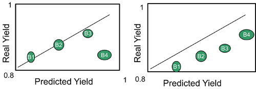
Fig 11.9 Actual (measured) yield vs predicted (based on design) yield in (a) case where a block is sensitive to process (b) case when defect level is more than the estimated value.
If we realize that a block is sensitive (Fig. 11.9a) can we find out which layer is failing? We can plot the measured yield vs layer sensitivity (i.e. critical area or via count or contact count) for all the blocks. Fig. 11.10 shows an example for yield plotted via count. The same analysis should be repeated for all layers. The layers for which B4-yield falls away from the line are sensitive to the process. This can help in narrowing down the processes which are suboptimal.
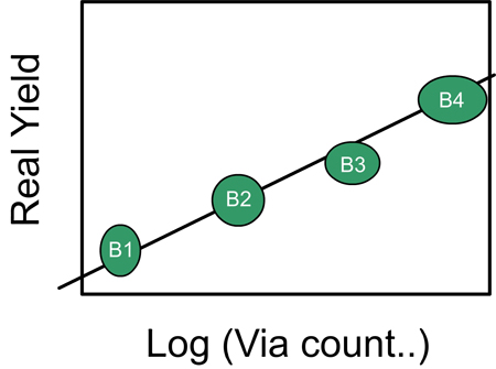
Fig. 11.10 . Plot of measured yield vs number of single via (or critical area of each layer)
Equipment commonality analysis: During the process, the wafers are passed though many equipment. At any particular stage (e.g. M1-lithography), there are usually more than one equipment available. If there are three litho equipment available, and in one lot, if there are 25 wafers, 8 wafers may pass though equipment-1, 8 may pass thorough equipment-2 and 9 may pass through equipment-3. If one of the equipments (e.g. equipment-2) is not controlled well, then the wafers passing through this may show poorer yield compared to other wafers in the same batch. In order to identify the problem, the yield of a wafer (or a block) and the equipment that it passed through must be compared. This analysis is called as equipment commonality analysis. This can be done only when we have sufficiently large quantity of test data. If we find that the wafers passing through one equipment consistently show poorer yield than wafers passing through other similar equipment, then we can take actions to rectify the problem.
Yield vs scribe line: In the test section, we learnt that some test structures on the outside of chips are also tested in parametric testing. This is also called scribe line testing or kerf testing. They show the resistance of small lines or leakage current of small structures in the wafer. Usually only a few sites on the wafer are tested. This information can also be used to identify certain type of failures. Sometimes a chip may fail, if the resistance of lines (connecting certain transistors) is high. The lines may not be open, (i.e. completely broken), but may just be of high resistance. These fails are sometimes called ‘soft opens’ while a completely broken line will be called ‘hard open’.
If the resistance of the lines in the chip are high, it is likely that the resistance of lines in the nearby scribe-line are also high. A plot of yield of the chips vs the resistance values measured in the scribe-lines nearby can indicate the issue. In Fig. 11.11, the schematic shows that when the scribeline resistance is high, the chip yield is low. This may be for scribeline in Metal 2. In that case, we can identify that metal-2 process needs to be optimized. Similar plots of yield vs scribeline parameters (such as M1, M3…resistance, leakages at various levels etc) can help identify the root cause of failures.
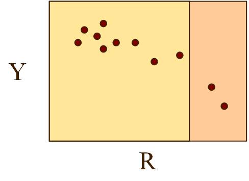
Fig. 11.11. Yield vs resistance of scribe-line.
11.8 Process and design modification for yield enhancement
If the yield is low because a particular layer or structure is systematically (repeatedly) failing, then either the process or the design or both can be modified to minimize failure. Two examples can illustrate this idea. In the first case, if metal 1 resistance is found to be higher than originally planned and if this is causing failures in some chips, then the ‘height’ of the metal 1 layer can be increased. This essentially increases the cross sectional area, without changing anything in the layout (design). In case of Cu interconnect, this means that the dielectric layer must be thicker, the etch must also be deeper and that the Cu deposition process must be able to deposit well in the trenches which are deeper now. This is an example of process modification to improve the yield.
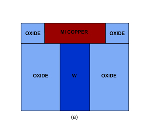 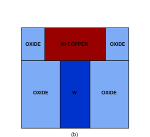
 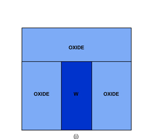
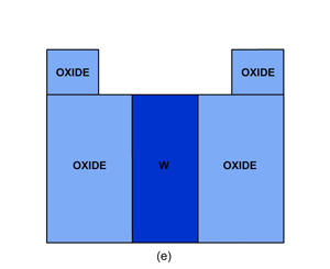 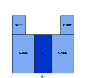
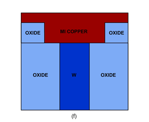 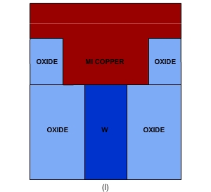
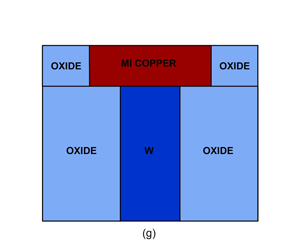 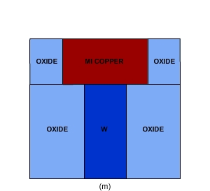
Figure 11.12 showing Cu layers with different heights. Fig. 11.12 (a) shows Cu with less height (thickness), and 11.12 (B) with more height. Compare two processes (b-g vs i-k), with extra oxide, deeper etch and deposition followed by CMP.
In second example, consider the formation of an ‘isolated’ line (i.e. a metal line without any neighboring lines in the next few micron distances) in aluminum interconnects. In this case, the photo resist will ideally appear exactly over the line, as shown in Fig. 11.13. However, due to non idealities in lithography, the actual line may be shorter than expected. In some designs, many chips may fail specifically because of this issue. The lines which have neighbors may not be affected to this extent because of interference effects. In this case, the best solution is to extend the length of isolated lines a bit in the layout itself. This is a design change that can enhance the yield. Here, the process remains the same but the layout (and hence the mask) is changed.
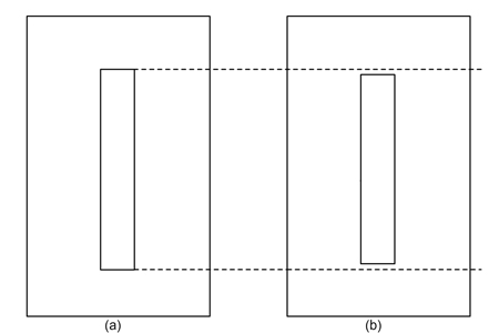
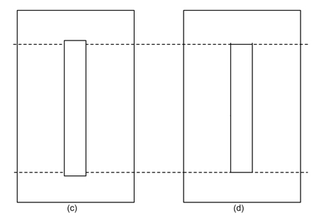
Fig. 11.13. Iso line, ideal case, iso line, actual case; iso line with mask modified.
Summary: Not all the chips in a wafer pass all the tests. The ratio of the number of passing chips to the total number of chips is called the yield. The chips can fail due to random defects falling on the wafer or due to sub optimal process or design. The yield loss due to random defect can be estimated using a knowledge of defect level and the sensitivity of the chip. The sensitivity is measured using a parameter called critical area and also using the number of single vias/contacts.
From the test data, which is usually measured in the SOF mode, the COF yield can be calculated and compared with the predicted yield. Various analyses such as overlay of wafer maps, block yield analysis and scribe line analysis can help in identifying the source of the problem. Once the problem is identified, either the process or the design can be modified to increase the yield.
|