For actual chips, the critical area is not analytically calculated using the layout. The circuits are very complex and a thorough and complete analysis of the layout is not practical. Hence, a few areas of the chip on the layout are chosen randomly and only 2 or 3 % of the chip area is used in the analysis. The critical area is calculated by simulating the occurrence of a defect (of a particular size) in a random location within these areas. This method of randomly ‘throwing’ defects and estimating the critical area falls under the category of Monte Carlo simulation.
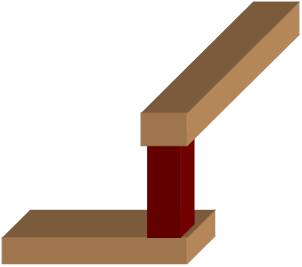 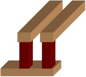
Fig. 11.4. Example of single via and redundant vias
In a chip, all the contacts are made in one size. Similarly, for a given via layer (e.g. Via23), all vias are made in the same size. Usually Via12 is the smallest and vias at the upper levels are larger. In order to calculate the yield of a contact layer or a via layer, instead of critical area, the the number of single vias (or single contacts) is used. A ‘single via’ is one which, if it fails, can cause the failure of the chip. In some locations, if large metal lines are used, then more than one via is used to connect the bottom metal to top metal. These are called ‘redundant vias’, as opposed to the ‘single’ vias, and the array of vias is called ‘via bank’. It is unlikely for a defect to cause the failure of all the vias in a via-bank. Hence only single vias are used to calculate the sensitivity of the via-layer to defects.
We know that the large defect can cause lot of problem. But number of the large defects in a good fab will be low. If we combine these two information, we understand the small size defects are more but they will not cause significant problem because the corresponding critical area is low. Large size defects will cause severe problem, (because the corresponding critical area is high) but there are a very few large defects in the fab. The medium size defects can cause problem to a moderate extent and there are moderate number of them present. Hence the yield loss usually comes from medium size defects in a fab. Of course if there are large size defects in the fab due to poor maintenance, the yield loss will be severe.
11.4 Models:
Crude model based on area: Even without taking into account the defect levels such as the defect size distribution, one may be able to roughly predict the yield for a chip. This is using the formula 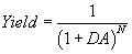 where D is the defect level, A is the area and N is called the complexity of the chip. If the chip has many metal layers (e.g. 7 or 8 layers) it is more difficult to make. Even if there is a problem in only one layer, the chip will fail and more number of layers would mean that the yield will be lower. Similarly, if the chip area is more then there is more probability of some defect falling within the area. Likewise if the defect level is more, it is also more likely to cause failure. However this model does not take the actual complexity of the chip (such as narrow lines vs wide lines, dense space vs sparse space etc). Usually, if there many chips are manufactured in a fab in one technology node, then the area of those chips and the number of metal layers on those chips are known. The yield of those chips would be available after testing. Based on these values, the value of D in the above formula can be calculated. For any new chip in the same technology node in the same fab, the formula can be used with that defect level, to quickly and approximately predict the yield. This method can not be used to predict the yield for a different technology node or in a different fab. where D is the defect level, A is the area and N is called the complexity of the chip. If the chip has many metal layers (e.g. 7 or 8 layers) it is more difficult to make. Even if there is a problem in only one layer, the chip will fail and more number of layers would mean that the yield will be lower. Similarly, if the chip area is more then there is more probability of some defect falling within the area. Likewise if the defect level is more, it is also more likely to cause failure. However this model does not take the actual complexity of the chip (such as narrow lines vs wide lines, dense space vs sparse space etc). Usually, if there many chips are manufactured in a fab in one technology node, then the area of those chips and the number of metal layers on those chips are known. The yield of those chips would be available after testing. Based on these values, the value of D in the above formula can be calculated. For any new chip in the same technology node in the same fab, the formula can be used with that defect level, to quickly and approximately predict the yield. This method can not be used to predict the yield for a different technology node or in a different fab.
The yield of the chip can be estimated more accurately from knowledge of the defect level (i.e. defect size distribution and fail rate) and complexity of the chip (i.e. critical area and the number of single vias/contacts). There are different models on the distribution of defect density (i.e. how many defects will fall on unit area).
In general, if the probability that a location on wafer will have a defect density of ‘x’ is given by P(x) and the probability that a location with that defect density will pass is given by Y(x), then the total yield is given by 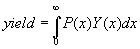 , with the constraint that , with the constraint that 
Poisson Model: If the defect density distribution is uniform (e.g. the defect density is 2 defects/cm2), then P(x) is given by d(2), where d is the delta function. The yield for a contact (via) layer is given by e-kN where k is the fail rate and N is the number of single contacts (vias).
On the other hand, the yield of a metal layer is given by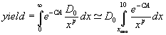
Note that the critical area (CA) is a function of defect size (x). Also, any defect of less than certain size (xmin) will not cause any yield loss and hence the lower limit of the integral is changed from 0 to xmin. On the other hand, random defects of size larger than 10 microns are NOT usually present in a fab and hence the upper limit is changed from infinity to 10 m. The model is anyway applicable only for random defects and if any large defects come from a specific equipment, the yield predictions are not applicable. Failures caused by sub-optimal processes and dust coming from specific equipment are called “systematic” instead of random. The Poisson model is often used in the industry because of its simplicity. It is reasonably valid when the defectivity is low and the predictions are actually a bit pessimistic. If there is strong spatial signal (i.e. if there is lot of defect at the center or lot of defects at the edges) then the Poisson model is not appropriate.
Seeds model: Here it is assumed that the defect density decreases exponentially, as shown in figure 10.5. The estimates from this model are usually optimistic. The seed model is more applicable if there are a lot of clusters of defects. Here clusters mean a group of defects which fall near the same location. The Poisson model and Seeds model results can be used as bounds for the yield estimates. The other models that have been proposed for the defect density are Murphy’s triangular distribution (which is a crude approximation for Gaussian distribution) and rectangular distribution. The model equations are given by
Seed model:  and and 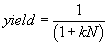
Murphy’s triangular model: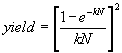 and Murphy’s rectangular model and Murphy’s rectangular model 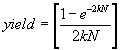
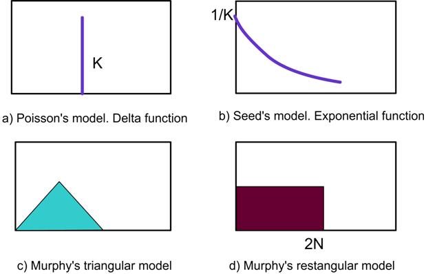 Fig. 11.5 Defect density distributions of (a) Poisson’s model (b) Seeds model (c ) Murphy’s triangular model and (d) Murphy’s rectangular model Fig. 11.5 Defect density distributions of (a) Poisson’s model (b) Seeds model (c ) Murphy’s triangular model and (d) Murphy’s rectangular model
Usually these are not employed since the calculations are more complicated than that of Poisson model and the accuracy of predictions are not significantly better.
Another empirical formula used for yield prediction is called the gamma model which is shown in the equation here. It does not have a physical basis and yet it is sometimes used because of its ability to predict yield reasonably well under different conditions.
In this model, if the parameter a has a value of 1, it becomes Seeds model (clustered), when it is 4.2, it is roughly similar to Murphy’s model and when it is infinity, it becomes the Poisson’s model. Thus it covers the entire range of clustering. The parameter a is called randomness of defects.
11.5 Defect types:
Not all the particles (defects) that fall on the wafer cause the failure of a circuit. For example if the particle falling on the lines is a electrically conducting material (Fig. 11.6a), then it will cause short circuit and the circuit will fail. Hence, this defect is called ‘killer’ defect. But if the defect is an insulator (Fig 11.6b), then it will not cause a failure. This type of defect is called “benign’ defect.
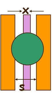 
Fig. 11.6. (a) Defect particle is a conducting material - killer defect (b) Defect particle is an insulator – benign defect.
11.6 Testing strategies
When the process is completed, the chip is tested (just before packaging) and we learnt about the sort test in the testing section. The usual mode of testing is called ‘stop on fail’ (SOF). When a chip fails a particular test, it is thrown into the corresponding bin. Now it is known that a particular part in the chip has failed. The failing chip is not subjected to the next test. Hence it is not known whether it will pass the next test or not. So, we do not know if the other untested parts of the chip are functioning properly or not.
The failing chip is not tested further because it is considered a waste of time. However, occasionally some of the failing chips will be tested further to identify all the failing parts of the chip. This method of testing is called ‘Continue on fail’ (COF), since the testing continues even after the chip fails in one or more tests.
Usually, when a new chip /design is brought into a fab, there will be difficulties in obtaining good yield. The yield may be less than 10% in the startup. After optimizing the design and process, the yield may increase to 60-80% depending on the design and the fab conditions. In the beginning of production, only a few wafers will be run with the new design so that maximum effort can be exerted to identify the design and process issues. At that time, COF testing is conducted. When most of the process and design issues are rectified, the yield increases; the chip is produced in large volume (i.e. many wafers are run). At that time, the testing is conducted in SOF mode, in order to save time.
|