11.1 Introduction:
In this chapter we will learn about yield which is a key parameter in chip manufacturing. If we try to make hundred chips and if only ninety of the chips pass all the tests, then the yield will be 90%. Ideally, we want to get 100% yield. But normally, for memory chips, the yield is > 95% and for processor chips, the yield will be in 50 to 80% if the process and design are reasonable. We will learn the following: 1. Understand the quantitative relationship between defect size and the yield loss 2. Predict the yield of a chip using the design (layout) details and the defect level of a fab 3. Understand different analyses used to identify the main cause of chip failure (root cause analysis), so that the fab can take suitable remedial action.
11.2 Defectivity: A parameter which is closely associated with yield is called defectivity. It indicates the level of defects in a fab. The chips are manufactured in clean rooms, but even in clean rooms, it is not possible to maintain 100 % cleanliness and there will always be small defects or particles floating around. Some of them will settle on the wafer during the process. The size distribution of these defects is important. Both the defect size distribution (DSD) and the number of defects are very important parameters.
First we will learn about Defect Size Distribution which is commonly called DSD. In a well maintained clean room, the defects of very small size will be more in numbers and large defects will be less and less. i.e. the defect level will decrease with particle size. The schematic shown below (Fig. 11.1) describes the defect density (i.e. number of defects per unit area) and the size of the defect.
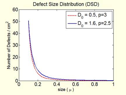
Fig. 11.1. Typical defect size distribution in a fab. A lower value of ‘p’ indicates more large defects
For a given circuit design, very small defects (below a certain value called critical dimension) will not cause any problem. This is usually given by the minimum space between the lines or the minimum width of a line or the size of a VIA or contact. The defect size distribution shown in Fig.11.1 is modeled by the equation
where D0 and p are the two parameters and x represents the size. For a good fabrication unit with good clean room facility, the value of p will typically be about 3, and defect density D0 should be less than 0.5/cm2. This model is valid for random defects. When the value of ‘p’ is lower than 3, it indicates that there are disproportionately high number of large defects.
While the defect size distribution is used to calculate the yield for metal layers, a different parameter called ‘fail rate’ is used to calculate the yield of contact or via layer. Here, it is assumed that each defect will cause only one via to fail. The fail rate is expressed in ‘parts per billion’ (ppb) vias and for a good fab it must be less than 0.5 ppb.
11.3 Critical Area: When the defects fall on the area, they will not always cause failure. Some locations on the chip are sensitive and if defects fall on them, it will cause failure. If the defects fall on other areas, they will not cause any problem. The quantification of this ‘sensitive’ area is critical area. If a chip has large critical area, it means that it is very sensitive to defects. If the fab has large defectivity, it is more likely to cause failure.
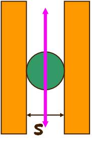
Consider two metal lines which are separated by a distance of 65 nm, as shown in Fig. 11.2. These two metals lines are separated by insulator. If the metal lines are short circuited, then the circuit will fail. Imagine that a small round defect of size ‘x’ falls on the chip. Let us also assume that the defect is a electricity conducting material. If its size is 40 nm, then regardless of where it falls, it will not cause any failure (Fig. 11.2b). Thus the chip is not sensitive to a defect of 40 nm. The critical area (CA) corresponding to 40 nm is zero.
Fig. 11.2
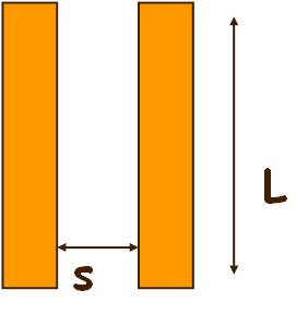
- Two metal lines separated by 65 nm distance
b. A defect of 40 nm, falling in many places on the chip
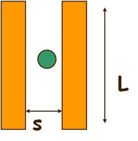
c. A defect of 65+ nm falling exactly on a particular line on the chip
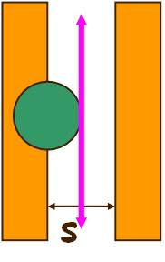
d. A defect of 65+ nm, falling randomly on the chip
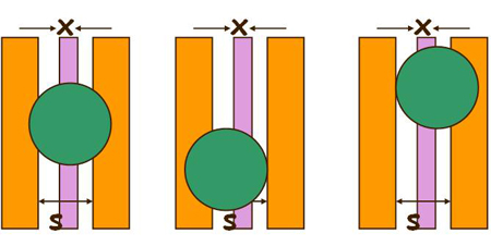
e. A defect of 90 nm, falling on ‘sensitive’ area of the chip
If the defect size is just above 65 nm, then the chip will fail only when the defect falls exactly in a particular line (Fig 11.2c). If the defect falls in any other area, then it will not cause any failure (Fig 11.2d). Thus the critical area corresponding to 65+ nm is just above zero. If the defect size is 90 nm, then the defect can fall in a fairly large area (Fig. 11.2e) and the destroy the chip. The CA is high. Based on this example, we can visualize that the critical area for shorts for a particular layer (e.g. Metal2) vs defect size will qualitatively appear as shown in Fig. 11.3
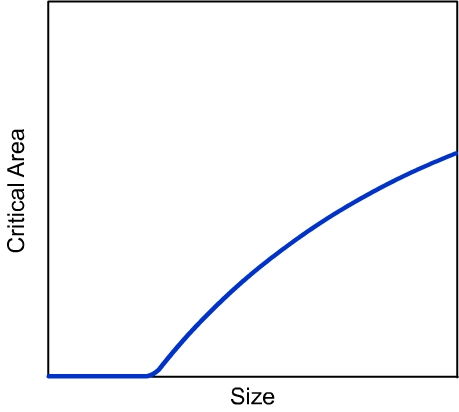
Fig 11.3 A qualitative plot of critical area vs defect size.
|