11.7 Yield analysis, root cause identification
Yield estimation from design: If the design data and defect level data are available, how does one estimate the yield? Consider the following example: A chip has four blocks called 1. SCAN, 2. PLL, 3. embedded DRAM, 4. ROM and 5. analog, as shown in figure 11.7. In terms of the layers, it has transistor, metal 1, metal 2 and metal 3, along with contacts, via12, via23. Please note that this is a simplified illustration. The areas not covered by the four blocks (PLL, DRAM, ROM or analog) is called SCAN. The ‘block view’ arises from the electrical circuit design. In the design stage and in operation, each block has a function and the name of the block is usually based on the functionality. There is another way to look at the chip and that is the layer view. During manufacturing, each layer is made one by one and the layers (metal 1 or M1, via12 or V12 etc) are shown in the schematic 11.7 b.
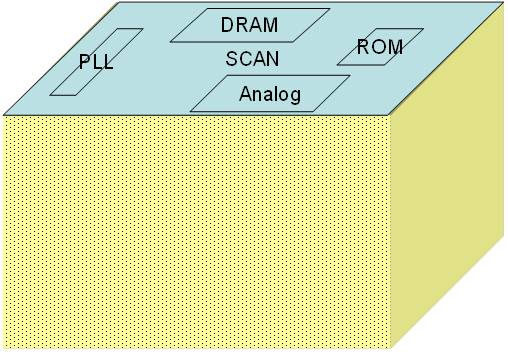
Fig 11.7a. Block view of the chip
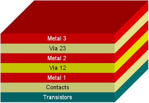
Fig 11.7b, layer view of the same chip
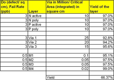
The critical area of each block, for each layer can be extracted from the layout information. The defect level can be obtained by using electrical test chips or optical defect inspection. Using these information, the yield by layer, for each block (and hence for the total chip) can be obtained.
An example of the calculation is given for the entire chip with four blocks and four metal layers in the table below. Please note that the ‘transistor’ layer is further divided into ‘N-Active’, ‘N-poly’ etc to account for source, drain and gate layers in NMOS and PMOS transistors.
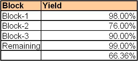
The overall yield is obtained by multiplying the yield of the individual layers. The same can be done at block level also. i.e. for each block, the critical area and the counts of contacts and vias in that block, should be calculated and the yield obtained using Poisson or other suitable model. The block level yields, when multiplied together, should also give the same chip yield as calculated by the ‘layer level’ yield. The ‘four block’ chip used in the previous table is analyzed using block level yield and illustrated in the table below.
The table tells the yield of each block if random defects are the only cause of failure. On the other hand, if some of the processes are not optimal, it is quite possible that only some of the blocks are affected more. In that case, the yield of those blocks will be poor. The calculations shown in the table are for COF testing. However, we know that usually in the fab SOF testing is done during mass production. We can estimate the COF results from SOF data as follows.
Yield calculation from bin data (sort data):Assume that 50 chips are tested using SOF strategy and each test (corresponding to each block) shows certain number of chips failing. The chips which pass all the tests are the ‘good’ chips.
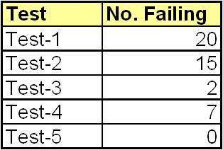
Thus, total number of good chips = 6 out 50. The COF yield (also called limited yield) can be estimated as shown below. After each test, the passing chips are used for the next test. Thus, the ‘total number’ of chips tested in test-2 is only 30. Out of 30 chips, 15 are failing. This indicates that if we have tested all 50 chips with test-2, 25 of them would have failed. Similarly, only 15 chips are subjected to test 3 and only 13 chips are subjected to test 4. Out of 13 chips, 7 have failed, indicating that the pass rate is about 47%. Thus, out of all the five blocks, block-4 has the lowest yield. This is not obvious by looking at SOF data alone.
Yield data analysis:
If the yield calculated from design and that from sort data match well, then it is clear that all the yield loss comes from random defects only. Any improvement in yield can arise only by improving the cleanliness of the fab. If the actual fab yield is less than the predicted yield, then we have to identify where the yield loss is coming from and rectify the problem. The yield loss coming from either a poor design or a poor process is called systematic yield loss. In that case, the following questions arise: 1. Is the problem related to one or more processes? 2. Is the problem related to one equipment? 3. Is the design (layout) sensitive to small variations in the process? In order to answer these questions, the yield data is presented in a few different perspectives. The yield data should also be compared with defect data and electrical parameter test data.
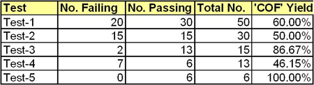
Creation of wafer maps: The yield of a wafer along with the location of the chip on the wafer is created. In Fig. 11.8a, many chips (dies) on the edge of the wafer fail, while the failures are less in the center of the wafer. If most wafers in a lot (of 10 or 13 or 25 wafers) show similar pattern, then, it indicates that some process shows non uniform behavior. E.g. In CMP, the edge may be polishing faster than the center. Or slurry particles may not be cleaned properly after CMP. Or, the Cu deposition process may deposit more at the edge than at the center. Many such hypothesis are possible, since the number of processes for making the chip is large.
Fig. 11.8. Wafer map of (a) yield (b) defect in litho chamber (c) defect in etch chamber
Overlay: The defect level in the fab is often monitored using dummy wafers, in various process chambers. The wafermap showing defects (e.g. Fig. 11.8b and 11.8c) should be compared with the yield map. In litho process, Fig. 11.8b shows that there is a large number of defects at the center. However, the yield map (Fig. 11.8a) shows that the chips at the center are passing all the tests. Hence we can conclude that the defects seen in litho process are benign defects. On the other hand, the defects in the etch chamber (Fig.11.8c) are more at the edge and they may be causing the yield loss.
Correlation between block yields
Based on the layout and defect level information, the yield of each block in a chip predicted. Based on the SOF test data, the COF yield can be estimated for each block. These two data sets can be compared by plotting the block yields of predicted vs actual values. If some blocks do not fall on the 45° line (Fig. 11.9a) , then we can conclude that the particular block is affected strongly by some process and hence the yield is poor for the block (B4 in this example). The layout should be analyzed and any significant difference between the affected block and other blocks, in terms of layout, must be carefully noted. Then either the process must be optimized to handle the layout part in the failing block and/or the layout must be modified slightly so that the block is less sensitive to process variations. The modification should not alter the main electronic circuit behavior though.
If the comparison shows that all the blocks lay below the 45° line (Fig. 11.9b) , then we can conclude that the defect level estimation is probably not correct and that the fab actually has more defects than estimated first.
|