Introduction: In a chemical industry, the temperature, pH and pressure of a liquid in a pipeline may be measured using thermocouple, pH probe and a pressure gauge respectively. The concentration of a chemical may be detected using techniques such as UV-Visible spectroscopy. In semiconductor industry, the tools and techniques used are different and a brief overview of some of them is presented here.
Scanning Electron Microscopy (SEM). This can be visualized as a very powerful microscope which can magnify the sample by more than 100000 times. Optical microscopes are capable of magnifying only up to 1000 times and diffraction of the light limits the resolution. The wavelength of the visible light is in the 400 – 700 nm region. Hence objects (or features) of smaller size can not be ‘seen’ using visible light.
Can we use shorter wavelength? Waves with wavelength lower than 400 nm are called ultra violet (UV). When the wavelength is less than 300 nm, it is called deep UV (DUV). Waves with wavelength of 100 to 10 nm are called extreme UV (EUV) and below 10 nm are called X Rays. If we use X Rays diffraction limitation will not be an issue. If the features are larger than 100 nm, EUV also will not suffer from diffraction limitations. However, EUV is absorbed by almost all materials, and X Ray will penetrate most of the materials. To obtain a usable image, a clear contrast must be generated and it is not possible to get one using EUV or X Ray. Hence electrons are used for imaging.
According to wave-particle duality all materials exhibit wave and particle properties. An electron, moving at high speeds, exhibits wave properties that are noticeable. Specifically, it behaves like a wave with a very short wavelength. Thus the diffraction limited resolution of such a ‘wave’ will be very good. This is the principle of SEM. A simplified schematic of an SEM is given below.
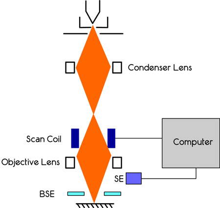
Figure 12.1. Schematic of SEM showing electron gun, condenser lens, sample, XY coils, secondary electron detector, back scattered electron detector, X ray detector.
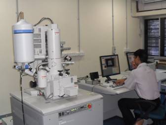
Fig. 12.2. A photo of Hitachi S-4800 model SEM (Courtesy, Department of Chemical Engineering, IIT-Madras).
Description: The SEM consists of an electron gun (which is the electron source), a electron condenser lens to control the size of the electron beam, a XY defection coils to move the electron beam in a controlled fashion, and detectors. At the minimum, an electron detector called ‘secondar electron detector’ is present. Usually backscattered electron detector and x-ray detectors are also found in most of the modern SEMs. The entire chamber is in ultra high vacuum.
Electron Gun: The electron gun can be a tungsten filament which emits electrons. More expensive electron guns use lanthanum hexaborate (LaB6). For these, the hot filament produces electrons by thermionic emission, which are used for image. A different type of electron source called Field Emission Gun(FEG) is used for very high magnification. SEM with FEG are usually called High Resolution SEM (HRSEM). In this type, the source is not heated by the current; instead, an electric field is used to obtain the electrons from the source, which is a very sharp tungsten crystal or zirconium oxide. The electrons will have an energy between 1 to 40 keV.
Condensing Lens: All the electrons are negatively charged and hence the electrons in a beam will repel each other. This will increase the beam diameter and will adversely affect the resolution of the image. Hence electrical coils are used to squeeze the beam to a diameter of 5 nm or less. These are called condensing lens coils.
Deflection coils: There are many differences between the SEM and optical microscopes, in terms of the techniques used. An electron beam is NOT used in the same way as light in optical microscope. In light microscope, the entire sample (or the region of interest) is illuminated simultaneously. In SEM, only one tiny spot is ‘illuminated’ with the beam. Then the beam is moved in small steps (usually in nm) by a process called ‘rastering’. This is similar to moving electron beam in a cathode ray tube (CRT). By applying suitable electric field, the beam can be made to ‘walk’ in the X and Y direction. The entire sample is analyzed by scanning the electron beam. Hence the instrument is called scanning electron microscope. The coils used for moving the electron beam are called deflection coils.
Interaction between ebeam and sample: When the electron beam falls on the sample, it will interact with the atoms and the electron will be slowed down due to strong elastic scattering. The atoms will absorb the energy and get ionized. Some of the electrons from the sample atoms will be released. These are called ‘secondary electrons’ (Figure 12.3) . They usually have lower energy (< 50 eV) compared to the primary electrons from the electron gun.
When the electron beam falls on the surface, the electrons are scattered and the beam diameter increases. Hence, in the beginning it spreads like a cone and the area below the surface also is probed. The beam energy decreases as it goes deeper inside the sample. The number of secondary electrons produced also decreases.
Besides, the electrons from the surface easily escape and arrive at the detector. The electrons from the bottom (trough) may be captured by other atoms before they escape to the surface. Hence only fewer secondary electrons from the trough come to the detector. Overall, the secondary electrons at the detector are essentially produced at the top of the surface.
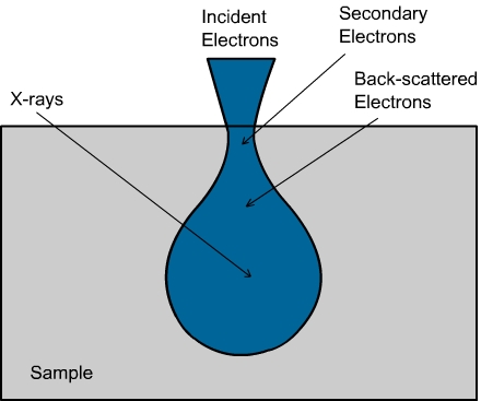
Figure 12.3 : A schematic of various possible results of electron hitting a sample. Secondary electrons, back scattered electrons and X Rays can be emitted as a result of the electron-sample interaction.
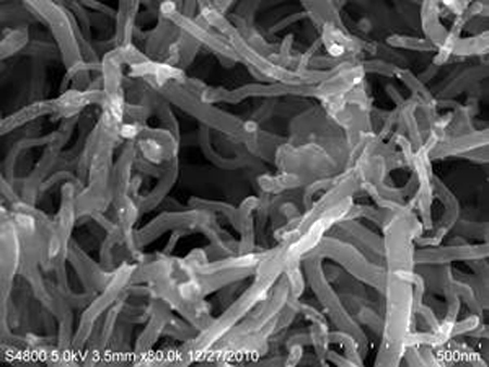
Figure 12.4: A SEM image of carbon nanotubes. (Courtesy, Department of Chemical Engineering, IIT-Madras).
Detectors:
The secondary electron is detected using a high performance detector.
X Ray detectors: EDS and WDS: The composition of the sample can be obtained using X ray detector. Two different techniques can be employed, viz. Energy dispersive X ray Spectroscopy (EDS or EDAX) or wavelength dispersive X ray spectroscopy (WDS).
When the electrons strike the atoms, sometimes the electron in the inner shell will be ejected out. Then, an electron from the outer shell will fall into the inner shell and the difference in energy will be emitted as X Rays (Figure 12.5). The energy difference is unique for each such transition and each element. Each element can give rise to many such transitions. If a K shell vacancy is filled by and L shell electron, the X ray is called K-alpha X Ray. If the K shell vacancy is filled by an M shell electron, it is called K-beta X ray. The characteristic X Rays are produced in a tear drop shaped region, as shown in Figure 12.3. By monitoring the X Ray, one can determine the composition of the surface. Usually the analysis is done for K, L and M shell electrons. Elements below carbon (in the periodic table) are difficult to detect. The accuracy is not very high and the composition is usually detectable only to within 1 atomic %. The advantage is that a very small sample size is sufficient.
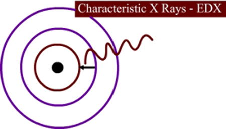
Figure 12.5 Illustration of energy levels and emission of characteristics X Rays in SEM
Normally the X Ray detector must be kept at a low temperature and this is achieved by using liquid nitrogen (which has a boiling point of about -200 C). Recently, detectors without using liquid nitrogen are also introduced and are sometimes called as ‘dry’ EDS detectors.
If the X Rays arrive one by one, then the detector will measure the energy of each X Ray photon and record it. Based on the energy values, we can determine which element is present on the sample. Based on the frequency of such occurrence, we can determine the composition (e.g. If X Ray corresponding to Si is observed 70 times and X ray corresponding to oxygen is observed 145 times, then we can say that the surface contains silicon and twice as much oxygen, i.e. SiO2). Hence it is called Energy Dispersive X Ray spectroscopy or EDS. One of the difficulties in this method is that if two X Rays arrive more or less at the same time, then the total energy of these photons will be recorded and it can lead to incorrect result.
An alternative to EDS is wavelength dispersive X Ray spectroscopy (WDS). In this, the XRays coming from the surface will be passed thorough a diffraction grating and only X Rays corresponding to one element will be allowed to go to the detector. Then, for a given time (e.g. 2 minutes), the number of photons at that wavelength arriving at the detector will be monitored. Next, the grating will be moved and X Rays corresponding to another element will be allowed to go to the detector. In this configuration, it takes significantly longer time to analyze a sample, but a more accurate determination of the composition is possible. In most cases, the accuracy obtained by EDS is sufficient and WDS is used only in special circumstances.
|